
User`s manual

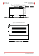
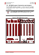


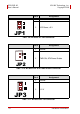

Table Of Contents
- ECS-8582-4S
- Revision History
- Preface
- Table of Contents
- List of Figures
- List of Tables
- 1 Introduction
- 2 Getting Started
- 3 Hardware Information
- 3.1 Functional Block Diagram
- 3.2 EC-8560
- 3.3 PCI-8565 Layout, Connectors and Jumpers
- 3.4 RK-8005 4-Slot Extension Chassis
- 3.5 BP-8005 Layout, Connectors and Jumpers
- Figure 3-7: BP-8005 Backplane Layout
- Table 3-4: BP-8005 Connectors, Jumpers and LED
- Table 3-5: BP-8005 CN1 LED Connector
- Table 3-6: BP-8005 CN2 ATX Power Connector
- Table 3-7: BP-8005 CN3 Fan Connector
- Table 3-8: BP-8005 CN4 ATX Power OK Status Connector
- Table 3-9: BP-8005 JP1 LED Connector
- Table 3-10: BP-8005 JP2 ATX Power Enable Connector
- Table 3-11: BP-8005 JP3 Fan Connector
- 3.6 Extension Cable Options
- 4 Troubleshooting (FAQ)
- Important Safety Instructions
- Warranty Policy
Hardware Information 23
ADLINK Technology, Inc. ECS-8582-4S
Copyright 2008 User’s Manual
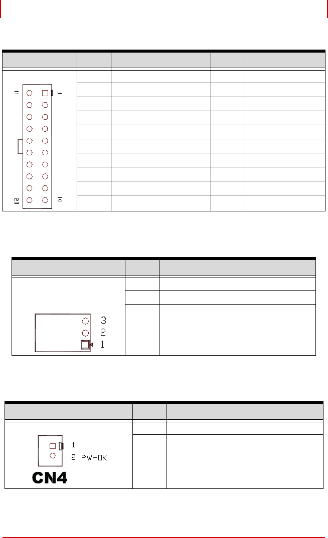
Table 3-6: BP-8005 CN2 ATX Power Connector
Table 3-7: BP-8005 CN3 Fan Connector
Table 3-8: BP-8005 CN4 ATX Power OK Status Connector
Pin # Assignment Pin # Assignment
1 +3.3 V 11 +3.3 V
2 +3.3 V 12 -12 V
3 Ground 13 Ground
4 +5 V 14 PS-ON
5 Ground 15 Ground
6 +5 V 16 Ground
7 Ground 17 Ground
8PW-OK 18-5 V
9 5 VSB 19 +5 V
10 +12 V 20 +5 V
Pin # Assignment
1N/C
2 +12 V
3 Ground
Pin # Assignment
1 Ground
2 PW-OK. ATX Power Status
CN2
CN3