
User`s guide


Operation Theory • 41
The D/A conversion is initiated by a trigger source. Users must decide how
to trigger the D/A conversion. The data output will start when a trigger
condition is met. Before the start of D/A conversion, D/A data is transferred
from PC’s main memory to a buffering Data FIFO.
There are two modes of the D/A conversion: Software Update and Timed
Waveform Generation are described, including timing, trigger source con-
trol, trigger modes and data transfer methods. Either mode may be ap-
plied to D/A channels independently. You can software update DA CH0
while generate timed waveforms on CH1 at the same time.
4.2.1 Software Update
This is the easiest way to generate D/A output. First, users should specify
the D/A output channels, set output polarity: unipolar or bipolar, and ref-
erence source: internal 10V or external AOEXTREF. Then update the
digital values into D/A data registers through a software output command.
4.2.2 Timed Waveform Generation
This mode can provide your applications with a precise D/A output with a
fixed update rate. It can be used to generate an infinite or finite waveform.
You can accurately program the update period of the D/A converters.
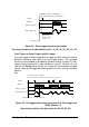
The D/A output timing is provided through a combination of counters in the
FPGA on board. There are totally 5 counters to be specified. These
counters are:
UI_counter(24 bits): specify the DA Update Interval =
CHUI_counter/Timebase.
UC_counter(24 bits): specify the total Update Counts in a single
waveform
IC_counter(24 bits): specify the Iteration Counts of waveform.
DLY1_counter(16 bits): specify the Delay from the trigger to the first
update start.
DLY2_counter(16 bits): specify the Delay between two consecutive
waveform generations.
Figure 22 shows the typical D/A timing diagram. D/A updates its output on
each rising edge of DAWR. The meaning of the counters above is dis-
cussed more in the following sections. For more information of Timebase,
please refer to 4.1.2.1.