
User`s guide


APDCAM User’s Guide
Page 18/32
At the beginning of the register map some registers describe the program and hard-
ware versions and the unique serial number of the ADC board.
After power-up the red-green bicolor ADC LED is lit green on the camera backplate.
If the ADC unit encounters a fatal problem this LED is red.
The DAQ unit is attached to the analog output signals at the backside of the detector
housing. The 32 input channels have an analog bandwidth of about 3 MHz, the input
voltage range is 0-2V. The input channels are grouped into 8-channel blocks, each block
is served by an 8-channel pipeline ADC chip. Data from one block is sent to one data
stream on the Gigabit communication card. The four streams are sent in separate UDP
datagrams on a single Gigabit connection to separate software ports in the PC.
3.3.1. ADC Timing
The timing is identical for all 32 channels and it is based on a single clock. This can be
either an internal 20 MHz oscillator or an external clock (clock in). Selection is done with
bit 0 in the CONTROL register. The external clock frequency is multiplied/divided by a
PLL (see CLOCK_PLL_MULT, CLOCK_PLL_DIV), therefore different input clock
frequencies can be accommodated in the 1...40 MHz range. The base clock generated
from the external clock should be between 19 and 40 MHz.
The ADC clock is generated from the selected base clock with a PLL (see
ADC_PLL_MULT, ADC_PLL_DIV), the resulting ADC clock must be between 10 and
50 MHz. An additional limitation is that the base clock multiplied by ADC_PLL_MULT
should be between 400 and 1000 MHz.
The status of the PLL units can be read from the STATUS1 and STATUS2 registers.
This is important especially if external clock is used. The external clock PLL status is
also shown on the camera backplate by the green Ext. Clock LED.
The 8-channel ADC blocks have a built-in test pattern generator which can be acti-
vated individually for all 4 blocks using the ADC_TEST_MODE register. This forces all
8 channels in one block to send the same test pattern.
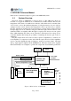
3.3.2. Filtering, resampling and channel selection
The ADCs generate a data stream with 32x14 bits. A digital filter can be enabled in
the CONTROL register which filters all 32 channel data with identical settings. The lay-
out of one filter is shown in Figure 8. The 14 bit data is fed in from the left side. A 5-
stage FIR filter allows steep cut of the frequency band somewhat below the sampling
frequency of the ADC. An additional recursive filter is implemented after the FIR filter to
allow for lower frequency cut-off, albeit with less steep characteristic. The recursive filter
implementation with integer arithmetic deserves some attention as long integration times
can cause overflow in the data. To handle this situation some flexibility is provided at
the end of the filter where the output 8, 12 or 14 bit data is cut out: the location of the
output bits can be selected.
The following procedure is proposed for calculation of the filter coefficients. The de-
sired cutoff frequency of the recursive filter (f
rec
) should be selected. From this the CO-
EFF_06 is
COEFF_06=
ADCrec
ff
e
2
4096
.