
User`s guide


APDCAM User’s Guide
Page 15/32
The detector can be overloaded if high input light level is applied while the bias volt-
age is on. Although the detector and electronics is protected against overload under the
most unfavourable conditions about 0.4W heat can be generated in the detector which
might result in damage if present for an extensive time. To prevent damage the camera
electronics contains an overload protection function which switches off the detector bias
voltage if the output signal is above a limit for an adjustable time.
An additional measure to prevent overload is the two-step bias voltage switch-on pro-
cedure. When APDCAM is switched on the bias voltage is off. First a bias voltage enable
code should be written into the bias enable register and the voltage can be switched on
only after that. This procedure prevents accidental biasing die to any accidental software
error.
The detector is mounted on a temperature controlled tab. The reference temperature is
set in a register of the control module. This temperature can be either below or above the
environmental temperature. (The environmental temperature is measured on the base of
the camera and can be read from the register table.) Cooling the camera does not provide
specific advantage, but temperature changes affect the detector, therefore the aim of tem-
perature control is to provide a stable gain. 18 C is recommended for detector tempera-
ture as it is slightly below usual room temperature but it does not cause condensation of
air humidity on the detector. Please note that the temperature of the detector has an effect
on the gain as well. Applying the same bias voltage at lower temperature causes higher
gain. Please consult the Hamamatsu S8550 datasheet for details.
The analog electronics utilize two amplifier stages for each channel, their bandwidth is
from DC to a maximum frequency. Parameters of the first stage (feedback resistor and
capacitance) determine the bandwidth and also the noise level. For setting an optimal
Signal to Noise ratio some information on the expected light level is required. As default
the amplifier is set up for about 10
10
photons/s light level and 1 MHz bandwidth. For
considerable different conditions the amplifier should be mounted with different compo-
nents, therefore a rough estimation of the light level and required bandwidth is necessary
at manufacturing time.
The high sensitivity amplifiers and the detector bias current can cause some drift in the
signal DC level. In order to compensate for this the analog electronics is equipped with a
DC offset input which can be set for each channel individually in the data acquisition
unit. The analog signals are negative in response to the input light, therefore the DC off-
set should be set to a high positive value to fit the signal into the 0-2V range of the digi-
tizer.
The detector is mounted directly on to the analog amplifier circuit board and cooled by
a cooling tab. The whole unit is mounted inside an Aluminium housing. The temperature
of the detector, the analog electronics and the housing are measured.
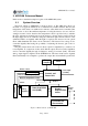
3.3. Data Acquisition Unit
The block scheme of the data acquisition unit (DAQ) is shown in Figure 7, while the
register map is in Table 5. and Table 6. After power-on different registers are set from
various sources as indicated in the table. Most of the registers recover their last data from
an on-board EEPROM memory, therefore they preserve their settings. Several of the reg-
isters will show the factory default value. This factory default can be regenerated for all