
Instruction manual


15
10 GB Communication
Version
1.0
3
& Control Card Instruction Manual
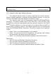
4.3 Clock management
The 10 GB C&C Card generates the ADC Clock (F4, 10-50 MHz), the
Sample Clock (F6) and the DSLV Reference Clock (FD1, 15-66 MHz) signals.
The ADC Clock and the Sample Clock are transmitted to the ADC boards
through the Control connector in LVDS format.
Figure 4. Clocking structure
The Serial PLL can be programmed using the PROGRAMSERIALPLL
instruction. FD1 is generated from the internal 20 MHz crystal oscillator. The
Serial PLL Multiply Value is 33 by default. (Note: FD1 and the DSLV clock
frequency of the ADC Board must be met.)
1 = 20 ×
(20. .50)
0(8. .100)
The Basic PLL can be programmed using the PROGRAMBASICPLL
instruction. F1 and FD1 are generated from the internal 20 MHz crystal
oscillator. The Basic PLL Multiply Value is 33 by default.
1 = 20 ×
(20. .50)
1(8. .100)
The lock status of the PLLs can be read out from the VARIABLES ACK (FPGA
Status byte).
The ADC Clock (F4) can be generated from internal (F1) or external
(F3) source. The Selector can be programmed by the SETCLOCKCONTROL
instruction. When external clock signal is used the Selector has two different
modes: normal and auto. In Auto External Clock Mode the Selector