
Datasheet


Electrical characteristics ST7LITE20F2 ST7LITE25F2 ST7LITE29F2
150/170 DocID8349 Rev 7
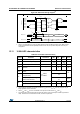
Figure 92. Amplifier noise vs voltage
13.11.1 Amplifier output offset variation
The offset is quite sensitive to temperature variations. In order to ensure a good reliability in
measurements, the offset must be recalibrated periodically i.e. during power on or whenever
the device is reset depending on the customer application and during temperature variation.
Table 87 gives the typical offset variation over temperature.
Table 86. ADC characteristics
(1)
1. Data based on characterization results over the whole temperature range, not tested in production.
Symbol Parameter Conditions Min Typ Max Unit
V
DD(AMP)
Amplifier operating voltage − 3.6 − 5.5 V
V
IN
Amplifier input voltage
(2)
2. Please refer to the application note AN1830 for details of TE% vs V
in
.
V
DD
=3.6V 0 − 350
mV
V
DD
=5V 0 − 500
V
OFFSET
Amplifier output offset
voltage
(3)
3. Refer to the offset variation in temperature below.
V
DD
=5V − 200 − mV
V
STEP
Step size for monotonicity
(4)
4. Monotonicity guaranteed if V
IN
increases or decreases in steps of min. 5mV.
V
DD
=3.6V 3.5 −−
mV
V
DD
=5V 4.89 −−
Linearity Output voltage response − Linear
Gain factor Amplified analog input gain
(5)
5. For precise conversion results, it is recommended to calibrate the amplifier at the following two points:
− offset at V
INmin
= 0V
− gain at full scale (for example V
IN
=430mV).
−−8 −−
Vmax Output linearity max voltage
V
INmax
= 430mV,
V
DD
=5V
− 3.65 3.94 V
Vmin Output linearity min voltage − 200 − mV
Vin
Vout (ADC input)
Vmax
Vmin
430mV
0V
Noise
(OPAMP input)
Table 87. Typical offset variation over temperature
Typical offset variation (LSB) Unit
-45 -20 +25 +90 °C
-12 -7 − +13 LSB