
Datasheet


Electrical characteristics ST7LITE20F2 ST7LITE25F2 ST7LITE29F2
148/170 DocID8349 Rev 7
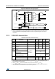
Figure 89. Typical application with ADC
5. The stabilization time of the AD converter is masked by the first t
LOAD
. The first conversion after the enable
is then always valid.
Table 85. ADC accuracy with V
DD
= 5.0V
Symbol Parameter Conditions Typ Max
(1)
1. Data based on characterization results over the whole temperature range, not tested in production.
Unit
|E
T
| Total unadjusted error
(2)
2. Injecting negative current on any of the analog input pins significantly reduces the accuracy of any
conversion being performed on any analog input.
Analog pins can be protected against negative injection by adding a Schottky diode (pin to ground).
Injecting negative current on digital input pins degrades ADC accuracy especially if performed on a pin
close to the analog input pins.
Any positive injection current within the limits specified for I
INJ(PIN)
and Σ
IINJ(PIN)
in Section 13.8: I/O port
pin characteristics does not affect the ADC accuracy.
f
CPU
=8MHz, f
ADC
=4MHz
(1)
, VDD=5.0V
36
LSB
|E
O
| Offset error
(2)
1.5 5
|E
G
| Gain Error
(2)
24.5
|E
D
|
Differential linearity
error
(2)
2.5 4.5
|E
L
| Integral linearity error
(2)
2.5 4.5
AINx
ST72XXX
V
DD
I
L
±1μA
V
T
0.6V
V
T
0.6V
C
ADC
6pF
V
AIN
R
AIN
10-Bit A/D
Conversion
C
AIN