
Datasheet


DocID8349 Rev 7 147/170
ST7LITE20F2 ST7LITE25F2 ST7LITE29F2 Electrical characteristics
169
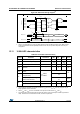
Figure 88. SPI master timing diagram
(1)
.
1. Measurement points are done at CMOS levels: 0.3xV
DD
and 0.7xV
DD
.
2. When no communication is on-going the data output line of the SPI (MOSI in master mode, MISO in slave
mode) has its alternate function capability released. In this case, the pin status depends on the I/O port
configuration.
13.11 10-Bit ADC characteristics
SS
INPUT
SCK
INPUT
CPHA=0
MOSI
OUTPUT
MISO
INPUT
CPHA=0
CPHA=1
CPHA=1
t
c(SCK)
t
w(SCKH)
t
w(SCKL)
t
h(MI)
t
su(MI)
t
v(MO)
t
h(MO)
MSB IN
MSB OUT
BIT6 IN
BIT6 OUT
LSB OUT
LSB IN
(2) (2)
CPOL=0
CPOL=1
CPOL=0
CPOL=1
t
r(SCK)
t
f(SCK)
Table 84. 10-bit ADC characteristics
(1)
1. Subject to general operating condition for V
DD
, f
OSC
, and T
A
unless otherwise specified.
Symbol Parameter Conditions Min Typ
(2)
2. Unless otherwise specified, typical data are based on T
A
=25°C and V
DD
-V
SS
=5V. They are given only as
design guidelines and are not tested.
Max Unit
f
ADC
ADC clock frequency −−−4MHz
V
AIN
Conversion voltage range
(3)
3. When V
DDA
and V
SSA
pins are not available on the pinout, the ADC refers to V
DD
and V
SS
.
− V
SSA
− V
DDA
V
R
AIN
External input resistor −−−10
(4)
4. Any added external serial resistor will downgrade the ADC accuracy (especially for resistance greater than
10kΩ) . Data based on characterization results, not tested in production.
kΩ
C
ADC
Internal sample and hold
capacitor
−−6 − pF
t
STAB
Stabilization time after ADC
enable
f
CPU
=8MHz,
f
ADC
=4MHz
0
(5)
μs
t
ADC
Conversion time
(Sample+Hold)
3.5
- Sample capacitor loading time
- Hold conversion time
4
10
1/f
ADC
I
ADC
Analog Part −−−1
mA
Digital Part −−−0.2