
Datasheet


Electrical characteristics ST7LITE20F2 ST7LITE25F2 ST7LITE29F2
146/170 DocID8349 Rev 7
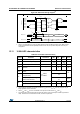
Figure 86. SPI slave timing diagram with CPHA = 0
(1)
1. Measurement points are done at CMOS levels: 0.3xV
DD
and 0.7xV
DD
.
2. When no communication is on-going the data output line of the SPI (MOSI in master mode, MISO in slave
mode) has its alternate function capability released. In this case, the pin status depends on the I/O port
configuration.
Figure 87. SPI slave timing diagram with CPHA = 1
(1)
1. Measurement points are done at CMOS levels: 0.3xV
DD
and 0.7xV
DD
.
2. When no communication is on-going the data output line of the SPI (MOSI in master mode, MISO in slave
mode) has its alternate function capability released. In this case, the pin status depends on the I/O port
configuration.
3. Depends on f
CPU
. For example, if f
CPU
= 8MHz, then T
CPU
= 1/ f
CPU
= 125ns and t
SU(SS)
= 550ns
SS
INPUT
SCK
INPUT
CPHA=0
MOSI
INPUT
MISO
OUTPUT
CPHA=0
t
c(SCK)
t
w(SCKH)
t
w(SCKL)
t
r(SCK)
t
f(SCK)
t
v(SO)
t
a(SO)
t
su(SI)
t
h(SI)
MSB OUT
MSB IN
BIT6 OUT
LSB IN
LSB OUT
CPOL=0
CPOL=1
t
su(SS)
t
h(SS)
t
dis(SO)
t
h(SO)
BIT1 IN
(2) (2)
SS
INPUT
SCK
INPUT
CPHA=0
MOSI
INPUT
MISO
OUTPUT
CPHA=0
t
w(SCKH)
t
w(SCKL)
t
r(SCK)
t
f(SCK)
t
a(SO)
t
su(SI)
t
h(SI)
MSB OUT BIT6 OUT
LSB OUT
CPOL=0
CPOL=1
t
su(SS)
t
h(SS)
t
dis(SO)
t
h(SO)
(2)
t
c(SCK)
HZ
t
v(SO)
MSB IN
LSB IN
BIT1 IN
(2)