
Datasheet


DocID8349 Rev 7 139/170
ST7LITE20F2 ST7LITE25F2 ST7LITE29F2 Electrical characteristics
169
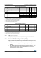
Figure 69. Typical V
OL
at V
DD
= 2.4V (standard)
Table 81. Output driving current
(1)
Symbol Parameter Conditions Min Max Unit
V
OL
(2)
Output low level voltage for a standard I/O
pin when 8 pins are sunk at same time
(see Figure 72)
V
DD
=5V
I
IO
=+5mAT
A
≤85°C
T
A
≥85°C
1.0
1.2
V
I
IO
=+2mAT
A
≤85°C
T
A
≥85°C
0.4
0.5
Output low level voltage for a high sink I/O
pin when 4 pins are sunk at same time
(see Figure 74)
I
IO
=+20mAT
A
≤85°C
T
A
≥85°C
1.3
1.5
I
IO
=+8mAT
A
≤85°C
T
A
≥85°C
0.75
0.85
V
OH
(3)
Output high level voltage for an I/O pin
when 4 pins are sourced at same time
(see Figure 80)
I
IO
=-5mAT
A
≤85°C
T
A
≥85°C
V
DD
-1.5
V
DD
-1.6
I
IO
=-2mAT
A
≤85°C
T
A
≥85°C
V
DD
-0.8
V
DD
-1.0
V
OL
(2)(4)
Output low level voltage for a standard I/O
pin when 8 pins are sunk at same time
(see Figure 71)
V
DD
=3.3V
I
IO
=+2mAT
A
≤85°C
T
A
≥85°C
0.5
0.6
Output low level voltage for a high sink I/O
pin when 4 pins are sunk at same time
I
IO
=+8mAT
A
≤85°C
T
A
≥85°C
0.5
0.6
V
OH
(3)(4)
Output high level voltage for an I/O pin
when 4 pins are sourced at same time
I
IO
=-2mAT
A
≤85°C
T
A
≥85°C
V
DD
-0.8
V
DD
-1.0
V
OL
(2)(4)
Output low level voltage for a standard I/O
pin when 8 pins are sunk at same time
(see Figure 69)
V
DD
=2.7V
I
IO
=+2mAT
A
≤85°C
T
A
≥85°C
0.6
0.7
Output low level voltage for a high sink I/O
pin when 4 pins are sunk at same time
I
IO
=+8mAT
A
≤85°C
T
A
≥85°C
0.6
0.7
V
OH
(3)(4)
Output high level voltage for an I/O pin
when 4 pins are sourced at same time
(see Figure 77)
I
IO
=-2mAT
A
≤85°C
T
A
≥85°C
V
DD
-0.9
V
DD
-1.0
1. Subject to general operating conditions for V
DD
, f
OSC
, and T
A
unless otherwise specified.
2. The I
IO
current sunk must always respect the absolute maximum rating specified in Table 58: Current characteristics and
the sum of I
IO
(I/O ports and control pins) must not exceed I
VSS
.
3. The I
IO
current sourced must always respect the absolute maximum rating specified in Table 58: Current characteristics
and the sum of I
IO
(I/O ports and control pins) must not exceed I
VDD
.
4. Not tested in production, based on characterization results.
0.00
0.10
0.20
0.30
0.40
0.50
0.60
0.70
0.01 1 2
lio (mA)
VOL at VDD=2.4V
-45
0°C
25°C
90°C
130°C