
Datasheet


DocID8349 Rev 7 137/170
ST7LITE20F2 ST7LITE25F2 ST7LITE29F2 Electrical characteristics
169
13.8 I/O port pin characteristics
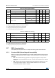
Table 79. Electrical sensitivities
Symbol Parameter Conditions Class
(1)
1. Class description: A Class is an STMicroelectronics internal specification. All its limits are higher than the
JEDEC specifications, that means when a device belongs to Class A it exceeds the JEDEC standard. B
Class strictly covers all the JEDEC criteria (international standard).
LU Static latch-up class T
A
=+25°C
A
DLU Dynamic latch-up class V
DD
=5.5V, f
OSC
=4MHz, T
A
=+25°C A
Table 80. General characteristics
(1)
1. Subject to general operating conditions for V
DD
, f
OSC
, and T
A
unless otherwise specified.
Symbol Parameter Conditions Min Typ Max Unit
V
IL
Input low level voltage − V
SS -
0.3 − 0.3 x V
DD
V
V
IH
Input high level voltage −
0.7 x
V
DD
− V
DD
+ 0.3
V
hys
Schmitt trigger voltage
hysteresis
(2)
2. Data based on characterization results, not tested in production.
−−400 − mV
I
L
Input leakage current V
SS
≤ V
IN
≤ V
DD
−−±1
μA
I
S
Static current consumption
induced by each floating input
pin
(3)
3. Configuration not recommended, all unused pins must be kept at a fixed voltage: using the output mode of
the I/O for example or an external pull-up or pull-down resistor (seeFigure 67). Static peak current value
taken at a fixed V
IN
value, based on design simulation and technology characteristics, not tested in
production. This value depends on V
DD
and temperature values.
Floating input mode − 400 −
R
PU
Weak pull-up equivalent
resistor
(4)
4. The R
PU
pull-up equivalent resistor is based on a resistive transistor (corresponding I
PU
current
characteristics described in Figure 68).
V
IN
=
V
SS
V
DD
=5V 50 120 250
kΩ
V
DD
=3V − 160 −
C
IO
I/O pin capacitance −−5 − pF
t
f(IO)out
Output high to low level fall
time
(2)
C
L
=50pF
Between 10% and
90%
− 25 −
ns
t
r(IO)out
Output low to high level rise
time
(2)
− 25 −
t
w(IT)in
External interrupt pulse time
(5)
5. To generate an external interrupt, a minimum pulse width has to be applied on an I/O port pin configured as
an external interrupt source.
− 1 −−t
CPU