
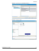
User guide


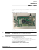
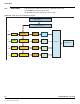

Demo kit Hardware Configuration
6-2 EV10AQ190x-DK - User Guide
1067BX–BDC–12/11
e2v semiconductors SAS 2011
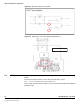
Figure 6-2. ADC Clock Selection Schematic
Figure 6-3. Implantation of R15, R37, R36 and R50 Resistors
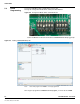
6.3 SPI Signal The SPI signal is controlled by the FX2 microcontroller, but it could also be controlled by
FPGA.
The selection between the two clocks is done manually with a resistor.
Note: e2v doesn't provide the SPI controller FPGA code.
Remove R93, R95, R97, R99 and R101 resistors and solder R94, R96, R98, R100 and
R102 with a 0.
TOP VIEW