
User guide


General Overview
1-2 EV10AQ190x-DK - User Guide
1067BX–BDC–12/11
e2v semiconductors SAS 2011
This kit must be regarded as a tool, not a finished product. It allows the evaluation of
performance of the e2v component, design prototypes and debug software. It CANNOT
be resold as a finished product that must be compliant with local relevant regulations.
Its function is as a development system, demonstrating the performance of e2v semi-
conductors components and not as a final product available on general release.
Since this Development Kit is intended to be used on an industrial workbench and mod-
ified by the user to build his prototypes, NO WARRANTY OF ANY KIND can apply.
NO LIABILITY will be accepted by e2v, whatsoever may arise as a result of the use of
these boards.
All company and/or product names may be tradenames, trademarks and/or registered
trademarks of the respective owner with which they are associated.
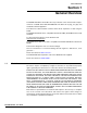
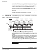
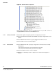
1.2 Quad 10-bit ADC The EV10AQ190x-DK Demo Kit is based on e2v EV10AQ190x 1.25 Gsps Quad 10-bit
ADC whose block diagram is given on Section 1-1.
Figure 1-1. EV10AQ190x Quad 10-bit ADC Block Diagram
The EV10AQ190x Quad 10-bit ADC integrates four 10-bit ADC cores which can operate
independently (four-channel mode) or group by two cores (two-channel mode with the
ADCs interleaved two by two) or one-channel mode where all four ADCs are all
interleaved.
All four ADCs are clocked from the same external input clock signal and controlled via
an SPI bus (Serial Peripheral Interface). An analog multiplexer (cross-point switch) is
used to select the analog input depending on the mode the quad ADC is used.
The clock input is common to all four ADCs. This block receives an external 2.5 GHz
clock (maximum frequency) and generates the internal sampling clocks for each ADC
core depending on the mode used. Please refer to latest version of datasheet
EV10AQ190x for more information.
http://www.e2v.com/products-and-services/specialist-semiconductors/broadband-data-
converters/datasheets/
Clock
Buffer
+
selection
+
decimation
+
SDA
LVDS Buffers
T/H
10 bit
1.25 Gsps
ADC core
10 bit
1.25 Gsps
ADC core
10 bit
1.25 Gsps
ADC core
10 bit
1.25 Gsps
ADC core
Analog MUX
(Cross Point Switch)
Serial
Peripheral
Interface
Offset
Gain
2.5 GHz
Clock
LVDS Buffers LVDS Buffers LVDS Buffers
Gain GainGain
T/H T/H T/H
Offset Offset Offset
Phase Phase Phase Phase