
User guide


Main Functions
EV10AQ190x-DK - User Guide 3-5
1067BX–BDC–12/11
3.3 Control of ADC
Settings
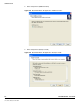
The Graphical User Interface allows for complete monitoring and control of all the set-
tings of EV10AQ190x Quad 10-bit ADC such as channel selection, Gain, Offset, Phase,
test mode (with SPI signal).
Please see Section 4.5 Operating Modes.
Please refer to datasheet EV10AQ190x for more information.
http://www.e2v.com/products-and-services/specialist-semiconductors/broadband-data-
converters/datasheets/
By default the SPI signal is controlled by FX2 microcontroller but it could be driven by
the FPGA. Please refer to Section 6.3 SPI Signal for more information.
3.4 ADC Junction
Temperature
Monitoring
ADC junction temperature can be monitored by a temperature sensor from ON Semi-
conductors Ref: ADM1032
http://www.onsemi.com/PowerSolutions/product.do?id=ADM1032
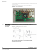
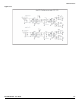
Figure 3-7. Temperature Sense: Schematic
ADC junction temperature can be displayed on the PC via the GUI with a resolution of
±2°C. Please see Section 4.5.5 Power.
In case of excessive junction temperature, the ADC power supply will be turned OFF
and a message will notify the user via the GUI.
The Demo Kit provides an external heat sink with internal fan
This heat sink should be fixed to the Quad 10-bit ADC with a thermal conductive foil
both side adhesive.
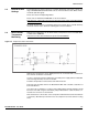
If no other form of ventilation or cooling is to be employed the heatsink ventilator should
be fixed to the ADC using the attachment pad provided and the cable should be con-
nected to the connector as shown below.
Note that because of the location of the component underneath the board a heatsink/fan
is necessary. Alternatively an airflow across the component can have sufficient cooling
effect.