
User guide


Main Functions
3-4 EV10AQ190x-DK - User Guide
1067BX–BDC–12/11
e2v semiconductors SAS 2011
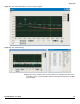
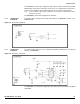
3.1.4 Analog Input
Channel D
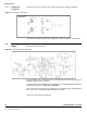
This channel is free for customer use in differential and AC coupling configuration.
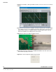
Figure 3-5. Channel D : Schematic
This Channel D could be used in DC configuration. Please see Section 6.1Channel D.
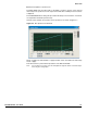
3.2 ADC Clock Input
Signal
ADC clock input is generated by Clock generated PLL Hititte HMC831 (on-board) at 2.0
GHz. This frequency is fixed.
Figure 3-6. ADC Clock Input : Schematic
Note: By default, the on-board PLL clock is selected but an external clock input (pro-
vided by a RF generator) is allowed.
The clock signal is fed to the board via an SMA connector followed by Single to Differen-
tial Balun RF transformer (MABA-007159 MACOM).
Note: for operation at different clock frequencies it is probable that the FPGA interface
will need to be re-compiled using different timing constraints.
Please see Section 6.2 Clock selection.