
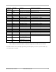
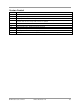
Specifications


© NXP Laboratories UK 2013 JN-DS-JN5148-001 1v9 95
Component
Designator
Value/Type Function PCB Layout Constraints
C13 10uF Power source decoupling
C14 100nF Analogue Power decoupling Adjacent to U1 pin 13
C16
100nF
Digital power decoupling
Adjacent to U1 pin 49
C15
100nF
VB Synth decoupling
Less than 5mm from U1 pin 10
C18
47pF
VB Synth decoupling
Less than 5mm from U1 pin 10
C2
10nF
VB VCO decoupling
Less than 5mm from U1 pin 12
C24
47pF
VB VCO decoupling
Less than 5mm from U1 pin 12
C3 100nF VB RF decoupling Less than 5mm from U1 pin 16 and U1 pin 18
C12 47pF VB RF decoupling Less than 5mm from U1 pin 16 and U1 pin 18
C8
100nF
VB A decoupling
Less than 5mm from U1 pin 27
C9
47pF
VB A decoupling
Less than 5mm from U1 pin 27
C6
100nF
VB RAM decoupling
Less than 5mm from U1 pin 35
C7
100nF
VB Dig decoupling
Less than 5mm from U1 pin 40
R1 43k I Bias Resistor Less than 5mm from U1 pin 14
C20 100nF Vref decoupling Less than 5mm from U1 pin 15
U2
4Mbit
Serial Flash Memory (Numonyx M25P40)
Y1
32MHz
Crystal (AEL X32M000000S025) (CL = 9pF, Max ESR 40R)
C10
15pF +/-5% COG
Crystal Load Capacitor
Adjacent to pin 8 and Y1 pin 1
C11
15pF +/-5% COG
Crystal Load Capacitor
Adjacent to pin 9 and Y1 pin 3
R2
Not fitted
C1 47pF AC Coupling
Phycomp 2238-869-15479
Must be copied directly from the reference design.
L1 5.6nH RF Matching Inductor
MuRata LQP15MN5N6B02
L2 2.7nH Load Inductor
MuRata LQP15MN2N7B02
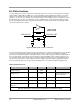
Table 8: JN5148 Printed Antenna Reference Module Components and PCB Layout Constraints
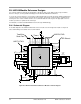
The paddle should be connected directly to ground. Any pads that requiring connection to ground should do so by
connecting directly to the paddle.