
Specifications


94 JN-DS-JN5148-001 1v9 © NXP Laboratories UK 2013
B.4 JN5148 Module Reference Designs
For customers wishing to integrate the JN5148 device directly into their system, NXP provide a range of Module
Reference Designs, covering standard and high-power modules fitted with different Antennae
To ensure the correct performance, it is strongly recommended that where possible the design details provided by the
reference designs, are used in their exact form for all end designs, this includes component values, pad dimensions,
track layouts etc. In order to minimise all risks, it is recommended that the entire layout of the appropriate reference
module, if possible, be replicated in the end design.
For full details, consult the Standard Module Reference Design JN-RD-6015 [6].
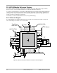
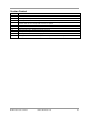
B.4.1 Schematic Diagram
A schematic diagram of the JN5148 PCB antenna reference module is shown in Figure 60. Details of component
values and PCB layout constraints can be found in Table 8.
1
2
3
4
5
6
7
8
9
10
11
12
13
14
15 16 17 18 19 20 21
22
23 24
25
26 27 28
29
30
31
32
33
34
35
36
37
38
39
40
41
42
434445464748
49
50515253545556
SPI Selects
Analogue IO
UART0/JTAG
Timers
Two Wire
Serial Port
RXD1
UART1/JTAG
DIO16
CTS1
VSS3
RTS1
TXD1
VSS2
VSSS
XTAL_OUT
XTAL_IN
VB_SYNTH
VCOTUNE (NC)
VB_VCO
R1 43K
IBIAS
C16 100nF
VDD1
C14 100nF
VDD
C13 10uF
C24 47pF
C18 47pF
C2 10nF
C15 100nF
Y1
C11 15pF
C10 15pF
C20 100nF
L2 2.7nH
VB_RF
VREF
VB_RF2
RF_IN
VB_RF
C3 100nF
C12 47pF
VB_RF1
C1M
C1P
ADC1
ADC2
ADC3
ADC4
C2M
C2P
VB_A
C9 47pF
C8 100nF
NC
VDD
VDD
RXD1
SPIMOSI
SPIMOSI
SPICLK
SPICLK
C6 100nF
C7 100nF
SPISEL3
SPISEL2
VB_DIG
RESETN
SPISEL1
SPISEL0
VB_RAM
SPIMISO
VSS1
DAC2
DAC1
1
2
3
4
8
7
6
5
SS
SD0
WP
VSS
SDI
CLK
HOLD
VCC
Serial
Flash
Memory
SPISEL4
CTS0
RTS0
TXD0
RXD0
VDD
VDD2
TIM0CK_GT
TIM0CAP
TIM0OUT
TIM1CK_GT
TIM1CAP
TIM1OUT
SIF_CLK
SIF_D
VSSA
JN5148
C1 47pF
L1 5.6nH
To Coaxial Socket
Or Integrated Antenna
Figure 60: JN5148 Printed Antenna Reference Module Schematic Diagram