
Specifications


88 JN-DS-JN5148-001 1v9 © NXP Laboratories UK 2013
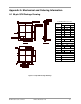
Appendix B Development Support
B.1 Crystal Oscillators
This section covers some of the general background to crystal oscillators, to help the user make informed decisions
concerning the choice of crystal and the associated capacitors.
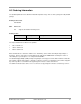
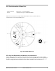
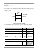
B.1.1 Crystal Equivalent Circuit
Cs
Lm
Cm
Rm
C2C1
Where
mC
is the motional capacitance
m
L
is the motional inductance. This together with
mC
defines the oscillation frequency (series)
mR
is the equivalent series resistance ( ESR ).
S
C
is the shunt or package capacitance and this is a parasitic
B.1.2 Crystal Load Capacitance
The crystal load capacitance is the total capacitance seen at the crystal pins, from all sources. As the load
capacitance (CL) affects the oscillation frequency by a process known as ‘pulling’, crystal manufacturers specify the
frequency for a given load capacitance only. A typical pulling coefficient is 15ppm/pF, to put this into context the
maximum frequency error in the IEEE802.15.4 specification is +/-40ppm for the transmitted signal. Therefore, it is
important for resonance at 32MHz exactly, that the specified load capacitance is provided.
The load capacitance can be calculated using:
CL
=
21
21
TT
TT
CC
CC
+
×
Total capacitance
inPT CCCC 1111
++=
Where
1C
is the capacitor component
P
C
1
is the PCB parasitic capacitance. With the recommended layout this is about 1.6pF
inC1
is the on-chip parasitic capacitance and is about 1.4pF typically.
Similarly for
2T
C
Hence for a 9pF load capacitance, and a tight layout the external capacitors should be 15pF