
Specifications


82 JN-DS-JN5148-001 1v9 © NXP Laboratories UK 2013
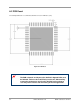
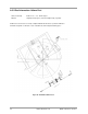
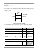
A.2 PCB Decal
The following PCB decal is recommended; all dimensions are in millimetres (mm).
Figure 52: PCB Decal
The PCB schematic and layout rules detailed in Appendix B.4 must
be followed. Failure to do so will likely result in the JN5148 failing
to meet the performance specification detailed herein and worst
case may result in device not functioning in the end application.