
Specifications


© NXP Laboratories UK 2013 JN-DS-JN5148-001 1v9 73
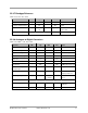
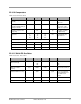
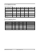
22.3.10 Comparators
VDD = 2.0 to 3.6V -40 to +85ºC
Parameter Min Typ Max Unit Notes
Analogue response time
(normal)
80 125 ns +/- 250mV overdrive
10pF load
Total response time
(normal) including delay to
Interrupt controller
105 + 125
ns
Digital delay can be
up to a max. of two
16MHz clock periods
Analogue response time
(low power)
2.4
µs +/- 250mV overdrive
No digital delay
Hysteresis 4
12
28
10
20
40
16
26
50
mV Programmable in 3
steps and zero
Vref (Internal)
See Section 22.3.7 Bandgap Reference
V
Common Mode input range 0 Vdd V
Current (normal mode)
54
73
102
µA
Current (low power mode)
0.8
µA
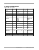
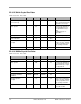
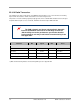
22.3.11 32kHz RC Oscillator
VDD = 2.0 to 3.6V, -40 to +85 ºC
Parameter Min Typ Max Unit Notes
Current consumption of cell
and counter logic
1.45
1.25
1.05
µA 3.6V
3.0V
2.0V
32kHz clock native
accuracy
-30%
32kHz
+30%
Typical is at 3.0V 25°C
Calibrated 32kHz accuracy ±250 ppm For a 1 second sleep
period calibrating over
20 x 32kHz clock
periods
Variation with temperature
-0.010
%/°C
Variation with VDD2
-1.1
%/V