
Specifications


72 JN-DS-JN5148-001 1v9 © NXP Laboratories UK 2013
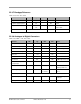
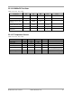
22.3.9 Digital to Analogue Converters
VDD = 3.0V, VREF = 1.2V, -40 to +85ºC
Parameter
Min
Typ
Max
Unit
Notes
Resolution
12
bits
Current consumption 215 (single)
235 (both)
µA
Integral nonlinearity
± 2
LSB
Differential nonlinearity
-1
+1
LSB
Guaranteed monotonic
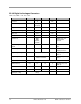
Offset error
± 10
mV
Gain error
± 10
mV
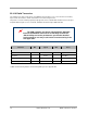
Internal clock 2MHz,
1MHz,
500kHz,
250kHz
16MHz input clock,
programmable
prescaler
Output settling time to
0.5LSB
5 µs With 10k ohms & 20pF
load
Minimum Update time 10 µs 2MHz Clock with
sample period of 2
Output voltage swing 0 Lower of Vdd-1.2 and Vref V Output voltage swing
Gain =0
Output voltage swing 0 Lower of 2x(Vdd-1.2 ) and
Vdd-0.2 and 2xVref
V Output voltage swing
Gain =1
Vref (Internal) See Section 22.3.7 Bandgap Reference
VREF (External) 0.8 1.2 1.6 V Allowable range into
VREF pin
Resistive load
10
kΩ
To ground
Capacitive load 20 pF
Digital input coding
Binary