
Specifications


© NXP Laboratories UK 2013 JN-DS-JN5148-001 1v9 71
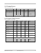
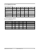
22.3.7 Bandgap Reference
VDD = 2.0 to 3.6V, -40 to +85ºC
Parameter Min Typ Max Unit Notes
Voltage
1.156
1.192
1.216
V
DC power supply rejection
58
dB
at 25ºC
Temperature coefficient -35
+30
ppm/ºC 20 to 85ºC
-40ºC to 20ºC
Point of inflexion
+25
ºC
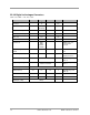
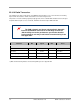
22.3.8 Analogue to Digital Converters
VDD = 3.0V, VREF = 1.2V, -40 to +85ºC
Parameter Min Typ Max Unit Notes
Resolution 12 bits 500kHz Clock
Current consumption
655
µA
Integral nonlinearity
± 5
LSB
0 to Vref range
Differential nonlinearity -1 +2 LSB Guaranteed monotonic
Offset error
+ 10
mV
Gain error
- 20
mV
Internal clock 500 kHz
16MHz input clock,
÷
32
No. internal clock periods
to sample input
2, 4, 6 or 8 Programmable
Conversion time
40
µs
500kHz Clock with
sample period of 2
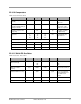
Input voltage range
0.04
Vref
or 2*Vref
V
Switchable. Refer to
20.1.1
Vref (Internal)
See Section 22.3.7 Bandgap Reference
Vref (External)
1.15
1.2
1.6
V
Allowable range into
VREF pin
Input capacitance
8
pF
In series with 5K ohms