
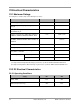
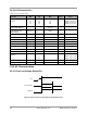
Specifications


© NXP Laboratories UK 2013 JN-DS-JN5148-001 1v9 69
Parameter Symbol Min Max Unit
Clock period
t
ck
125.0
-
ns
Data setup time
t
si
15
-
ns
Data hold time t
hi
15 ns
Data invalid period t
vo
- 40 ns
Select set-up period
t
sss
15
-
ns
Select hold period
t
ssh
15
-
ns
Select asserted to output data driven
t
lz
20
ns
Select negated to data output tri-stated
t
hz
20
ns
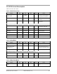
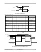
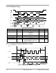
22.3.4 Two-wire Serial Interface
t
BUF
Sr P
SS
t
LOW
t
HD;STA
t
F
t
R
t
HD;DAT
t
HIGH
t
SU;DAT
t
SU;STA
t
HD;STA
t
SU;STO
t
SP
t
R
t
F
SIF_D
SIF_CLK
Figure 50: Two-wire Serial Interface Timing
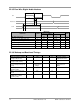
Parameter Symbol
Standard Mode Fast Mode
Unit
Min Max Min Max
SIF_CLK clock frequency
f
SCL
0 100 0 400 kHz
Hold time (repeated) START condition.
After this period, the first clock pulse is
generated
t
HD:STA
4 - 0.6 - µs
LOW period of the SIF_CLK clock
t
LOW
4.7 - 1.3 - µs
HIGH period of the SIF_CLK clock
t
HIGH
4 - 0.6 - µs
Set-up time for repeated START condition
t
SU:STA
4.7
-
0.6
-
µs
Data setup time SIF_D
t
SU:DAT
0.25
-
0.1
-
µs
Rise Time SIF_D and SIF_CLK
t
R
-
1000
20+0.1Cb
300
ns
Fall Time SIF_D and SIF_CLK
t
F
-
300
20+0.1Cb
300
ns
Set-up time for STOP condition
t
SU:STO
4
-
0.6
-
µs
Bus free time between a STOP and START
condition
t
BUF
4.7 - 1.3 - µs
Pulse width of spikes that will be
suppressed by input filters (Note 1)
t
SP
-
60
-
60
ns
Capacitive load for each bus line
C
b
-
400
-
400
pF
Noise margin at the LOW level for each
connected device (including hysteresis)
V
nl
0.1VDD
-
0.1VDD
-
V
Noise margin at the HIGH level for each
connected device (including hysteresis)
V
nh
0.2VDD - 0.2VDD - V
Note 1: This figure indicates the pulse width that is guaranteed to be suppressed. Pulse with widths up to 125nsec
may alos get suppressed.