
Specifications


© NXP Laboratories UK 2013 JN-DS-JN5148-001 1v9 67
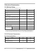
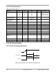
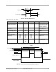
Internal RESET
RESETN
V
RST
t
STAB
t
RST
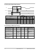
Figure 46: Externally Applied Reset
VDD = 2.0 to 3.6V, -40 to +85º C
Parameter Min Typ Max Unit Notes
External Reset pulse width
to initiate reset sequence
(t
RST
)
1
µs
Assumes internal pullup
resistor value of 100K
worst case and ~5pF
external capacitance
External Reset threshold
voltage (V
RST
)
VDD2 x 0.7
V
Minimum voltage to
avoid being reset
Internal Power-on Reset
threshold voltage (V
POT
)
1.47
1.42
V Rising
Falling
Reset stabilisation time
(t
STAB
)
0.84 ms Note 1
Brown-out Threshold
Voltage (V
TH
)
1.87
2.16
2.54
2.83
1.95
2.25
2.65
2.95
2.01
2.32
2.73
3.04
V
Configurable threshold
with 4 levels
Brown-out Hysteresis
(V
HYS
)
45
60
85
100
mV Corresponding to the 4
threshold levels
1
Time from release of reset to start of executing ROM code. Loading program from Flash occurs in addition to this.
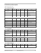
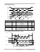
VTH + VHYS
VTH
DVDD
Internal POR
Internal BOReset
VPOT
Figure 47: Power on Reset followed by Brown-out Detect