
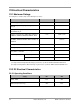
Specifications


66 JN-DS-JN5148-001 1v9 © NXP Laboratories UK 2013
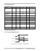
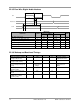
22.2.3 I/O Characteristics
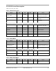
VDD = 2.0 to 3.6V, -40 to +85º C
Parameter Min Typ Max Unit Notes
Internal DIO pullup
resistors
22
24
31
35
34
40
56
63
53
63
92
104
kΩ
VDD2 = 3.6V, 25C
VDD2 = 3.0V, 25C
VDD2 = 2.2V, 25C
VDD2 = 2.0V, 25C
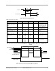
Digital I/O High Input
(except DIO9, DIO10)
VDD2 x 0.7 Lower of (VDD2 + 2V)
and 5.5V
V 5V Tolerant I/O only
Digital I/O High Input
( DIO9, DIO10)
VDD2 x 0.7 VDD2 V
Digital I/O low Input -0.3 VDD2 x 0.27 V
Digital I/O input hysteresis 140 230 310 mV
DIO High O/P (2.7-3.6V) VDD2 x 0.8 VDD2 V With 4mA load
DIO Low O/P (2.7-3.6V) 0 0.4 V With 4mA load
DIO High O/P (2.2-2.7V) VDD2 x 0.8 VDD2 V With 3mA load
DIO Low O/P (2.2-2.7V) 0 0.4 V With 3mA load
DIO High O/P (2.0-2.2V) VDD2 x 0.8 VDD2 V With 2.5mA load
DIO Low O/P (2.0-2.2V) 0 0.4 V With 2.5mA load
Current sink/source
capability
4
3
2.5
mA VDD2 = 2.7V to 3.6V
VDD2 = 2.2V to 2.7V
VDD2 = 2.0V to 2.2V
I
IL -
Input Leakage Current 50 nA Vcc = 3.6V, pin low
I
IH -
Input Leakage Current 50 nA Vcc = 3.6V, pin high
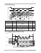
22.3 AC Characteristics
22.3.1 Reset and Voltage Brown-Out
RESETN
Internal RESET
VDD
V
POT
t
STAB
Figure 45: Internal Power-on Reset without showing Brown-Out