
Specifications


64 JN-DS-JN5148-001 1v9 © NXP Laboratories UK 2013
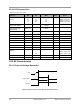
22 Electrical Characteristics
22.1 Maximum Ratings
Exceeding these conditions may result in damage to the device.
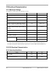
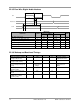
Parameter
Min
Max
Device supply voltage VDD1, VDD2
-0.3V
3.6V
Supply voltage at voltage regulator bypass pins
VB_xxx
-0.3V
1.98V
Voltage on analogue pins XTALOUT, XTALIN,
VCOTUNE, RF_IN.
-0.3V
VB_xxx + 0.3V
Voltage on analogue pins VREF, ADC1-4, DAC1-2,
COMP1M, COMP1P, COMP2M, COMP2P, IBIAS
-0.3V
VDD1 + 0.3V
Voltage on 5v tolerant digital pins SPICLK,
SPIMOSI, SPIMISO, SPISEL0, DIO0-8 & DIO11-20,
RESETN
-0.3V
Lower of (VDD2 + 2V)
and 5.5V
Voltage on 3v tolerant digital pins DIO9, DIO10
-0.3V
VDD2 + 0.3V
Storage temperature
-40ºC
150ºC
Reflow soldering temperature according to
IPC/JEDEC J-STD-020C
260ºC
ESD rating
4
Human Body Model
1
2.0kV
Charged Device Model
2
500V
1) Testing for Human Body Model discharge is performed as specified in JEDEC Standard JESD22-A114.
2) Testing for Charged Device Model discharge is performed as specified in JEDEC Standard JESD22-C101.
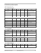
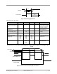
22.2 DC Electrical Characteristics
22.2.1 Operating Conditions
Supply Min Max
VDD1, VDD2 2.0V 3.6V
Ambient temperature range -40ºC 85ºC