
Specifications

58 JN-DS-JN5148-001 1v9 © NXP Laboratories UK 2013
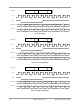
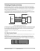
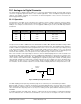
20 Analogue Peripherals
The JN5148 contains a number of analogue peripherals allowing the direct connection of a wide range of external
sensors, switches and actuators.
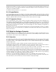
ADC
DAC1
DAC2
VREF
Chip
Boundary
Internal Reference
Processor Bus
Supply Voltage
(VDD1)
Vref select
Temp
Sensor
Comparator 2
Comparator 1
COMP2M
COMP1M
COMP1P
COMP2P
DAC1
DAC2
ADC1
ADC2
ADC3
ADC4
Vref
Figure 43: Analogue Peripherals
In order to provide good isolation from digital noise, the analogue peripherals are powered by a separate regulator,
supplied from the analogue supply VDD1 and referenced to analogue ground VSSA.
A common reference Vref for the ADC and DAC can be selected between an internal bandgap reference or an
external voltage reference supplied to the VREF pin. Gain settings for the ADC and DAC are independent of each
other.
The ADC and DAC are clocked from a common clock source derived from the 16MHz clock