
Specifications


© NXP Laboratories UK 2013 JN-DS-JN5148-001 1v9 41
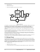
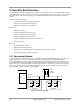
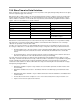
1 2 3 1 2 N
Conversion cycle 1
2
17
N
Conversion cycle 2
3
Figure 29: Return To Zero Mode in Operation
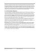
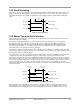
1 2 3 1 2 N
Conversion cycle 1
N 3
2
16
Conversion cycle 2
Figure 30: Non-Return to Zero Mode
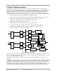
11.1.5 Example Timer / Counter Application
Figure 31 shows an application of the JN5148 timers to provide closed loop speed control. Timer 0 is configured in
PWM mode to provide a variable mark-space ratio switching waveform to the gate of the NFET. This in turn controls
the power in the DC motor.
Timer 1 is configured to count the rising edge events on the clk/gate pin over a constant period. This converts the
tacho pulse stream output into a count proportional to the motor speed. This value is then used by the application
software executing the control algorithm.
If required for other functionality, then the unused IO associated with the timers could be used as general purpose
DIO.
JN5148
Timer 0
Timer 1
CLK/GATE
CLK/GATE
CAPTURE
CAPTURE
PWM
PWM
M
Tacho
48
50
52
53
54
1N4007
+12V
IRF521
51
1 pulse/rev
Figure 31: Closed Loop PWM Speed Control Using JN5148 Timers
11.2 Tick Timer
The JN5148 contains a hardware timer that can be used for generating timing interrupts to software. It may be used
to implement regular events such as ticks for software timers or an operating system, as a high-precision timing
reference or can be used to implement system monitor timeouts as used in a watchdog timer. Features include:
• 32-bit counter