
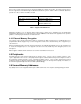
Specifications


© NXP Laboratories UK 2013 JN-DS-JN5148-001 1v9 11
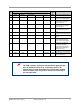
Pin
No
Digital Peripheral I/O
Signal
Type
Description
Primary Alternate Functions
51 DIO10 TIM0OUT 32KXTALOUT CMOS
DIO10, Timer0 PWM Output or
32K External Crystal Output
52 DIO11 TIM1CK_GT TIM2OUT CMOS
DIO11, Timer1 Clock/Gate
Input or Timer2 PWM Output
53 DIO12 TIM1CAP ADO DAI_WS CMOS
DIO12, Timer1 Capture Input,
Antenna Diversity or Digital
Audio Word Select
54 DIO13 TIM1OUT ADE DAI_SDIN CMOS
DIO13, Timer1 PWM Output,
Antenna Diversity or Digital
Audio Data Input
55 DIO14 SIF_CLK IP_CLK CMOS
DIO14, Serial Interface Clock
or Intelligent Peripheral Clock
Input
56 DIO15 SIF_D IP_DO CMOS
DIO15, Serial Interface Data or
Intelligent Peripheral Data Out
1 DIO16 IP_DI CMOS
DIO16 or Intelligent Peripheral
Data In
2 DIO17 CTS1 IP_SEL DAI_SCK JTAG_TCK CMOS
DIO17, UART 1 Clear To Send
Input, Intelligent Peripheral
Device Select Input or Digital
Audio Clock or JTAG CLK
4 DIO18 RTS1 IP_INT DAI_SDOUT JTAG_TMS CMOS
DIO18, UART 1 Request To
Send Output, Intelligent
Peripheral Interrupt Output or
Digital Audio Data Output or
JTAG Mode Select
5
DIO19
TXD1
JTAG_TDO
CMOS
DIO19 or UART 1 Transmit
Data Output or JTAG Data Out
31
DIO 20
RXD1
JTAG_TDI
CMOS
DIO 20, UART 1 Receive Data
Input or JTAG data In
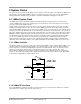
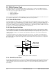
The PCB schematic and layout rules detailed in Appendix B.4
must be followed. Failure to do so will likely result in the
JN5148 failing to meet the performance specification detailed
herein and worst case may result in device not functioning in
the end application.