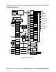
Data Sheet: JN5148-001 IEEE802.15.4 Wireless Microcontroller Features: Transceiver Overview The JN5148-001 is an ultra low power, high performance wireless microcontroller targeted at JenNet and ZigBee PRO networking applications. The device features an enhanced 32-bit RISC processor offering high coding efficiency through variable width instructions, a multistage instruction pipeline and low power operation with programmable clock speeds. It also includes a 2.4GHz IEEE802.15.
Contents 1 Introduction 6 1.1 Wireless Transceiver 1.2 RISC CPU and Memory 1.3 Peripherals 1.4 Block Diagram 6 6 7 8 2 Pin Configurations 9 2.1 Pin Assignment 2.2 Pin Descriptions 2.2.1 Power Supplies 2.2.2 Reset 2.2.3 32MHz Oscillator 2.2.4 Radio 2.2.5 Analogue Peripherals 2.2.6 Digital Input/Output 10 12 12 12 12 12 13 13 3 CPU 15 4 Memory Organisation 16 4.1 ROM 4.2 RAM 4.3 OTP eFuse Memory 4.4 External Memory 4.4.1 External Memory Encryption 4.5 Peripherals 4.
8 Wireless Transceiver 26 8.1 Radio 8.1.1 Radio External Components 8.1.2 Antenna Diversity 8.2 Modem 8.3 Baseband Processor 8.3.1 Transmit 8.3.2 Reception 8.3.3 Auto Acknowledge 8.3.4 Beacon Generation 8.3.5 Security 8.4 Security Coprocessor 8.5 Location Awareness 8.6 Higher Data Rates 26 27 27 29 30 30 30 31 31 31 31 31 32 9 Digital Input/Output 33 10 Serial Peripheral Interface 35 11 Timers 38 11.1 Peripheral Timer/Counters 11.1.1 Pulse Width Modulation Mode 11.1.2 Capture Mode 11.1.
20 Analogue Peripherals 58 20.1 Analogue to Digital Converter 20.1.1 Operation 20.1.2 Supply Monitor 20.1.3 Temperature Sensor 20.2 Digital to Analogue Converter 20.2.1 Operation 20.3 Comparators 59 59 60 60 60 60 61 21 Power Management and Sleep Modes 62 21.1 Operating Modes 21.1.1 Power Domains 21.2 Active Processing Mode 21.2.1 CPU Doze 21.3 Sleep Mode 21.3.1 Wakeup Timer Event 21.3.2 DIO Event 21.3.3 Comparator Event 21.3.4 Pulse Counter 21.
Appendix A Mechanical and Ordering Information 81 A.1 56-pin QFN Package Drawing A.2 PCB Decal A.3 Ordering Information A.4 Device Package Marking A.5 Tape and Reel Information A.5.1 Tape Orientation and Dimensions A.5.2 Reel Information: 180mm Reel A.5.3 Reel Information: 330mm Reel A.5.4 Dry Pack Requirement for Moisture Sensitive Material 81 82 83 84 85 85 86 87 87 Appendix B Development Support 88 B.1 Crystal Oscillators B.1.1 Crystal Equivalent Circuit B.1.2 Crystal Load Capacitance B.1.
1 Introduction The JN5148-001 is an IEEE802.15.4 wireless microcontroller that provides a fully integrated solution for applications using the IEEE802.15.4 standard in the 2.4 - 2.5GHz ISM frequency band [1], including JenNet and ZigBee PRO. It includes all of the functionality required to meet the IEEE802.15.
1.
1.
DIO3/SPISEL4/RFTX DIO4/CTS0/JTAG_TCK 44 43 DIO5/RTS0/JTAG_TMS 45 DIO6/TXD0/JTAG_TDO DIO8/TIM0CK_GT/PC 1 48 46 VDD2 49 DIO7/RXD0/JT AG_TDI DIO9/TIM0CAP/32KXT ALIN/32KIN 50 47 DIO10/T IM0OUT/32KXT ALOUT 51 DIO11/T IM1CK_GT /TIM2OUT 52 53 DIO12/T IM1CAP/ADO/DAI_WS DIO13/T IM1OUT/ADE/DAI_SDIN DIO14/SIF_C LK/IP_CLK 55 54 DIO15/SIF_D/IP_DO 56 2 Pin Configurations DIO16/RXD 1/IP_DI/JTAG_TDI DIO 16/IP_DI 1 42 DIO2/SPISEL3/RFRX DIO17/CTS1/IP_SEL/DAI_SC K/JTAG_TCK 2 41 DIO1/SPISEL2/PC0 VSS
2.1 Pin Assignment Pin No Power supplies Signal Type Description 10, 12, 16, 18, 27, 35, 40 VB_SYNTH, VB_VCO, VB_RF2, VB_RF, VB_A, VB_RAM, VB_DIG 1.8V Regulated supply voltage 13, 49 VDD1, VDD2 3.3V Supplies: VDD1 for analogue, VDD2 for digital 32, 6, 3, 7, Paddle VSS1, VSS2, VSS3, VSSS, VSSA 0V Grounds (see appendix A.2 for paddle details) 28 NC No connect General 39 RESETN 8, 9 XTAL_OUT, XTAL_IN CMOS 1.8V Reset input System crystal oscillator Radio 11 VCOTUNE 1.
Digital Peripheral I/O Signal Type Description 32KXTALOUT CMOS DIO10, Timer0 PWM Output or 32K External Crystal Output TIM1CK_GT TIM2OUT CMOS DIO11, Timer1 Clock/Gate Input or Timer2 PWM Output DIO12 TIM1CAP ADO DAI_WS CMOS DIO12, Timer1 Capture Input, Antenna Diversity or Digital Audio Word Select 54 DIO13 TIM1OUT ADE DAI_SDIN CMOS DIO13, Timer1 PWM Output, Antenna Diversity or Digital Audio Data Input 55 DIO14 SIF_CLK IP_CLK CMOS DIO14, Serial Interface Clock or Intelligent Per
2.2 Pin Descriptions 2.2.1 Power Supplies The device is powered from the VDD1 and VDD2 pins, each being decoupled with a 100nF ceramic capacitor. VDD1 is the power supply to the analogue circuitry; it should be decoupled to ground. VDD2 is the power supply for the digital circuitry; and should also be decoupled to ground. A 10uF tantalum capacitor is required. Decoupling pins for the internal 1.8V regulators are provided which require a 100nF capacitor located as close to the device as practical.
2.2.5 Analogue Peripherals Several of the analogue peripherals require a reference voltage to use as part of their operations. They can use either an internal reference voltage or an external reference connected to VREF. This voltage is referenced to analogue ground and the performance of the analogue peripherals is dependant on the quality of this reference. There are four ADC inputs, two pairs of comparator inputs and two DAC outputs. The analogue I/O pins on the JN5148 can have signals applied up to 0.
VDD2 Pu OE RPU O DIO[x] Pin RPROT I VSS IE Figure 4: DIO Pin Equivalent Schematic In reset, the digital peripherals are all off and the DIO pins are set as high-impedance inputs. During sleep and deep sleep, the DIO pins retain both their input/output state and output level that was set as sleep commences. If the DIO pins were enabled as inputs and the interrupts were enabled then these pins may be used to wake up the JN5148 from sleep.
3 CPU The CPU of the JN5148 is a 32-bit load and store RISC processor.
4 Memory Organisation This section describes the different memories found within the JN5148. The device contains ROM, RAM, OTP eFuse memory, the wireless transceiver and peripherals all within the same linear address space. 0xFFFFFFFF 0xF0020000 RAM (128kB) 0xF0000000 Unpopulated RAM Echo 0x04000000 Peripherals 0x02000000 0x00020000 ROM (128kB) 0x00000000 Figure 5: JN5148 Memory Map 4.1 ROM The ROM is 128k bytes in size, and can be accessed by the processor in a single CPU clock cycle.
4.2 RAM The JN5148 contains 128kBytes of high speed RAM. It can be used for both code and data storage and is accessed by the CPU in a single clock cycle. At reset, a boot loader controls the loading of segments of code and data from an external memory connected to the SPI port, into RAM. Software can control the power supply to the RAM allowing the contents to be maintained during a sleep period when other parts of the device are un-powered. Typical RAM contents are shown in Figure 7.
At reset, the contents of this memory are copied into RAM by the software boot loader. The Flash memory devices that are supported as standard through the JN5148 bootloader are given in Table 1. NXP recommends that where possible one of these devices should be selected.
5 System Clocks Two system clocks are used to provide timing references into the on-chip subsystems of the JN5148. A 16MHz clock, generated by a crystal-controlled 32MHz oscillator, is used by the transceiver, processor, memory and digital and analogue peripherals. A 32kHz clock is used by the sleep timer and during the startup phase of the chip. 5.1 16MHz System Clock The 16MHz system clock is used by the digital and analogue peripherals and the transceiver.
5.2 32kHz System Clock The 32kHz system clock is used for timing the length of a sleep period (see section 21 Power Management and Sleep Modes) and also to generate the system clock used internally during reset. The clock can be selected from one of three sources through the application software: • 32kHz RC Oscillator • 32kHz Crystal Oscillator • 32kHz External Clock Upon a chip reset or power-up the JN5148 defaults to using the internal 32kHz RC Oscillator.
6 Reset A system reset initialises the device to a pre-defined state and forces the CPU to start program execution from the reset vector. The reset process that the JN5148 goes through is as follows. When power is applied, the 32kHz RC oscillator starts up and stabilises, which takes approximately 100µsec. At this point, the 32MHz crystal oscillator is enabled and power is applied to the processor and peripheral logic.
VDD JN5148 R1 18k RESETN C1 470nF Figure 12: External Reset Generation The external resistor and capacitor provide a simple reset operation when connected to the RESETN pin. 6.2 External Reset An external reset is generated by a low level on the RESETN pin. Reset pulses longer than the minimum pulse width will generate a reset during active or sleep modes. Shorter pulses are not guaranteed to generate a reset. The JN5148 is held in reset while the RESETN pin is low.
6.4 Brown-out Detect An internal brown-out detect module is used to monitor the supply voltage to the JN5148; this can be used whilst the device is awake or is in CPU doze mode. Dips in the supply voltage below a variable threshold can be detected and can be used to cause the JN5148 to perform a chip reset. Equally, dips in the supply voltage can be detected and used to cause an interrupt to the processor, when the voltage either drops below the threshold or rises above it.
7 Interrupt System The interrupt system on the JN5148 is a hardware-vectored interrupt system. The JN5148 provides several interrupt sources, some associated with CPU operations (CPU exceptions) and others which are used by hardware in the device. When an interrupt occurs, the CPU stops executing the current program and loads its program counter with a fixed hardware address specific to that interrupt.
7.3 Hardware Interrupts Hardware interrupts generated from the transceiver, analogue or digital peripherals and DIO pins are individually masked using the Programmable Interrupt Controller (PIC). Management of interrupts is provided in the peripherals library [5]. For details of the interrupts generated from each peripheral see the respective section in this datasheet. Interrupts can be used to wake the JN5148 from sleep.
8 Wireless Transceiver The wireless transceiver comprises a 2.45GHz radio, modem, a baseband processor, a security coprocessor and PHY controller. These blocks, with protocol software provided as a library, implement an IEEE802.15.4 standardsbased wireless transceiver that transmits and receives data over the air in the unlicensed 2.4GHz band. 8.1 Radio Figure 14 shows the single ended radio architecture.
8.1.1 Radio External Components In order to realise the full performance of the radio it is essential that the reference PCB layout and BOM are carefully followed. See Appendix B.4. The radio is powered from a number of internal 1.8V regulators fed from the analogue supply VDD1, in order to provide good noise isolation between the digital logic of the JN5148 and the analogue blocks. These regulators are also controlled by the baseband controller and protocol software to minimise power consumption.
Antenna A Antenna B A ADO (DIO[12]) B SEL RF Switch: Single-Pole, Double-Throw (SPDT) ADE (DIO[13]) SELB COM Device RF Port Figure 16 Simple Antenna Diversity Implementation using External RF Switch ADE (DIO[13]) ADO (DIO[12]) TX Active RX Active 1st TX-RX Cycle 2nd TX-RX Cycle (1st Retry) Figure 17 Antenna Diversity ADO Signal for TX with Acknowledgement If two DIO pins cannot be spared, DIO13 can be configured to be a normal DIO pin, and the inverse of ADO generated with an inverter on th
8.2 Modem The modem performs all the necessary modulation and spreading functions required for digital transmission and reception of data at 250kbps in the 2450MHz radio frequency band in compliance with the IEEE802.15.4 standard. It also provides a high data rate modes at 500 and 667kbps.
8.3 Baseband Processor The baseband processor provides all time-critical functions of the IEEE802.15.4 MAC layer. Dedicated hardware guarantees air interface timing is precise. The MAC layer hardware/software partitioning, enables software to implement the sequencing of events required by the protocol and to schedule timed events with millisecond resolution, and the hardware to implement specific events with microsecond timing resolution.
provided to indicate successful packet reception. During reception, the modem determines the Link Quality, which is made available at the end of the reception as part of the requirements of IEEE802.15.4. 8.3.3 Auto Acknowledge Part of the protocol allows for transmitted frames to be acknowledged by the destination sending an acknowledge packet within a very short window after the transmitted frame has been received.
8.6 Higher Data Rates To support the demands of applications that require high data throughputs such as in audio or data streaming applications, the JN5148 supports higher data rate modes that offer 500kbps or 667kbps on air transmission rates. The switching between standard and higher data rates is controlled via software, When operating in a higher data rate mode standard IEEE802.15.4 features, such as clear channel assessment, can still be used.
9 Digital Input/Output There are 21 Digital I/O (DIO) pins, which can be configured as either an input or an output, and each has a selectable internal pull-up resistor. Most DIO pins are multiplexed with alternate peripheral features of the device, see section 2.1. Once a peripheral is enabled it takes precedence over the device pins. Refer to the individual module sections for a full description of the alternate peripherals functions.
SPICLK SPIMOSI SPIMISO SPI Master SPISEL0 SPISEL1 DIO0/SPISEL1 SPISEL2 DIO1/SPISEL2/PC0 SPISEL3 DIO2/SPISEL3/RFRX SPISEL4 DIO3/SPISEL4/RFTX TXD0 DIO4/CTS0/JTAG_TCK RXD0 UART0 DIO5/RTS0/JTAG_TMS RTS0 DIO6/TXD0/JTAG_TDO CTS0 DIO7/RXD0/JTAG_TDI TXD1 UART1 RXD1 DIO8/TIM0CK_GT/PC1 RTS1 DIO9/TIM0CAP/32KXTALIN/32KIN CTS1 DIO10/TIM0OUT/32KXTALOUT TIM0CK_GT Timer0 DIO11/TIM1CK_GT/TIM2OUT TIM0OUT DIO12/TIM1CAP/ADO/DAI_WS TIM0CAP DIO13/TIM1OUT/ADE/DAI_SDN TIM1CK_GT Timer1 DIO14/SIF_
10 Serial Peripheral Interface The Serial Peripheral Interface (SPI) allows high-speed synchronous data transfer between the JN5148 and peripheral devices. The JN5148 operates as a master on the SPI bus and all other devices connected to the SPI are expected to be slave devices under the control of the JN5148 CPU.
SS SO User Defined SI SS Slave 4 C SI SO User Defined C SS Slave 3 SO C SI C User Defined SO User Defined SI Slave 2 SS SS Slave 1 SO C SI Slave 0 Flash/ EEPROM Memory SPISEL 1 SPISEL 2 42 41 38 37 JN5148 43 SPISEL 3 SPISEL 4 SPISEL 0 36 SPIMOSI 33 SPICLK 34 SPIMISO Figure 24: Typical JN5148 SPI Peripheral Connection The data transfer rate on the SPI bus is determined by the SPICLK signal.
sent from a slave, it should perform transmit using dummy data. An interrupt can be generated when the transaction has completed or alternatively the interface can be polled. If a slave device wishes to signal the JN5148 indicating that it has data to provide, it may be connected to one of the DIO pins that can be enabled as an interrupt. Figure 25 shows a complex SPI transfer, reading data from a FLASH device, that can be achieved using the SPI master interface.
11 Timers 11.1 Peripheral Timer/Counters Three general-purpose timer/counter units are available that can be independently configured to operate in one of five possible modes. Timer 0 and 1 support all 5 modes of operation and Timer 2 supports PWM and Delta-Sigma modes only.
The clock source for the timer unit is fed from the 16MHz system clock. This clock passes to a 5-bit prescaler where a prescale value. For example, a prescale value of value of 0 leaves the clock unmodified and other values divide it by 2 2 applied to the 16MHz system clock source results in a timer clock of 4MHz. The counter is optionally gated by a signal on the clock/gate input (TIMxCK_GT). If the gate function is selected, then the counter is frozen when the clock/gate input is high.
9 5 4 3 CLK CAPT tRISE tRISE tFALL tFALL Capture Mode Enabled Rise x Fall 3 9 x 14 7 Figure 28: Capture Mode 11.1.3 Counter/Timer Mode The counter/timer can be used to generate interrupts, based on the timers or event counting, for software to use. As a timer the clock source is from the system clock, prescaled if required. The timer period is programmed into the Fall register and the Fall register match interrupt enabled.
1 2 3 N 1 2 3 N 217 Conversion cycle 1 Conversion cycle 2 Figure 29: Return To Zero Mode in Operation 1 2 3 N Conversion cycle 1 1 216 2 3 N Conversion cycle 2 Figure 30: Non-Return to Zero Mode 11.1.5 Example Timer / Counter Application Figure 31 shows an application of the JN5148 timers to provide closed loop speed control. Timer 0 is configured in PWM mode to provide a variable mark-space ratio switching waveform to the gate of the NFET.
• 28-bit match value • Maskable timer interrupt • Single-shot, Restartable or Continuous modes of operation Match Value = Match Tick Timer Interrupt & SysClk & Counter Reset Int Enable Run Mode Control Mode Figure 32: Tick Timer The Tick Timer is clocked from a continuous 16MHz clock, which is fed to a 32-bit wide resettable up-counter, gated by a signal from the mode control block. A match register allows comparison between the counter and a programmed value.
A wakeup timer consists of a 35-bit down counter clocked from the selected 32 kHz clock. An interrupt or wakeup event can be generated when the counter reaches zero. On reaching zero the counter will continue to count down until stopped, which allows the latency in responding to the interrupt to be measured. If an interrupt or wakeup event is required, the timer interrupt should be enabled before loading the count value for the period.
12 Pulse Counters Two 16-bit counters are provided that can increment during all modes of operation (including sleep), based on pulses received on 2 dedicated DIO inputs; DIO1 and DIO8. The pulses can be de-bounced using the 32kHz clock to guard against false counting on slow or noisy edges. Increments occur from a configurable rising or falling edge on the respective DIO input. Each counter has an associated 16-bit reference that is loaded by the user.
13 Serial Communications The JN5148 has two independent Universal Asynchronous Receiver/Transmitter (UART) serial communication interfaces. These provide similar operating features to the industry standard 16550A device operating in FIFO mode. Each interface performs serial-to-parallel conversion on incoming serial data and parallel-to-serial conversion on outgoing data from the CPU to external devices.
where the hardware controls the value of the generated RTS (negated if the receive FIFO fill level is greater than a programmable threshold of 8, 11, 13 or 15 bytes), and only transmits data when the incoming CTS is asserted. Software can read characters, one byte at a time, from the Receive FIFO and can also write to the Transmit FIFO, one byte at a time. The Transmit and Receive FIFOs can be cleared and reset independently of each other.
14 JTAG Debug Interface The JN5148 includes an IEEE1149.1 compliant JTAG port for the sole purpose of software code debug with NXP's Software Developer’s Kit. The JTAG interface is disabled by default and is enabled under software control. Therefore, debugging is only possible if enabled by the application. Once enabled, the application executes as normal until the external debugger controller initiates debug activity.
15 Two-Wire Serial Interface The JN5148 includes industry standard two-wire synchronous Serial Interface operates as a Master (MSIF) or Slave (SSIF) that provides a simple and efficient method of data exchange between devices.
15.2 Clock Stretching Slave devices can use clock stretching to slow down the transfer bit rate. After the master has driven SIF_CLK low, the slave can drive SIF_CLK low for the required period and then release it. If the slave’s SIF_CLK low period is greater than the master’s low period the resulting SIF_CLK bus signal low period is stretched thus inserting wait states. Clock held low by Slave SIF_CLK Master SIF_CLK SIF_CLK Slave SIF_CLK SIF_CLK Wired-AND SIF_CLK Figure 36: Clock Stretching 15.
15.4 Slave Two-wire Serial Interface When operating as a slave device, the interface does not provide a clock signal, although it may drive the clock signal low if it is required to apply clock stretching. Only transfers whose address matches the value programmed into the interface’s address register are accepted. The interface allows both 7 and 10 bit addresses to be programmed, but only responds with an acknowledge to a single address.
16 Four-Wire Digital Audio Interface The JN5148 includes a four-wire digital audio interface that can be used for interfacing to audio CODECs.
Data Buffer Right R2 R1 R0 Left L2 L1 L0 SCK Left Right WS SD Max Size MSB MSB-1 MSB-2 SD 3-bits L2 L1 L0 0 LSB MSB MSB-1 MSB-2 0 R2 R1 R0 LSB 0 0 Figure 38: I²S Mode Data Buffer Right R2 R1 R0 Left L2 L1 L0 SCK Left Right WS SD Max Size MSB MSB-1 MSB-2 SD 3-bits L2 L1 L0 0 LSB MSB MSB-1 MSB-2 0 R2 R1 R0 LSB 0 0 Figure 39: Left Justified Mode Data Buffer Right R2 R1 R0 Left L2 L1 L0 SCK Left Right WS SD Max Size MSB MSB-1 SD 3-bits 0 0
17 Random Number Generator A random number generator is provided which creates a 16-bit random number each time it is invoked. Consecutive calls can be made to build up any length of random number required. Each call takes approximately 0.25msec to complete. Alternatively, continuous generation mode can be used where a new number is generated approximately every 0.25msec. In either mode of operation an interrupt can be generated to indicate when the number is available, or a status bit can be polled.
18 Sample FIFO A 10 deep FIFO is provided to buffer data between the CPU and either the four-wire digital audio interface or the DAC/ ADC. It supports single channel input and output data, up to 16 bits wide. When used it can reduce the rate at which the processor has to generate/process data, and this may allow more efficient operation. Interrupts can be generated based on fill levels and also FIFO empty and full conditions.
19 Intelligent Peripheral Interface The Intelligent Peripheral (IP) Interface is provided for systems that are more complex, where there is a processor that requires a wireless peripheral. As an example, the JN5148 may provide a complete JenNet or ZigBee PRO wireless network interface to a phone, computer, PDA, set-top box or games console. No resources are required from the main processor compared to a transceiver as the complete wireless protocol may be run on the internal JN5148 CPU.
If data is queued for transmission and the recipient has indicated that they are ready for it (RXRDY in incoming status byte was 1), the next byte to be transmitted is the data length in words (N). If either the JN5148 or the remote processor has no data to transfer, then the data length should be set to zero. The transaction can be terminated by the master after the status and padding bytes have been sent if it is not possible to send data in either direction.
all the data specified in the length field to the JN5148. The master must then deassert IP_SEL to show the transfer is complete. The master may initiate a transfer to read data from the JN5148 by asserting the slave select pin, IP_SEL, and generating its status byte on IP_DI with RXRDY set. After receiving the status byte from the JN5148, it should check that the JN5148 has a buffer ready by reading the TXRDY bit of the received status byte.
20 Analogue Peripherals The JN5148 contains a number of analogue peripherals allowing the direct connection of a wide range of external sensors, switches and actuators.
20.1 Analogue to Digital Converter The 12-bit analogue to digital converter (ADC) uses a successive approximation design to perform high accuracy conversions as typically required in wireless sensor network applications. It has six multiplexed single-ended input channels: four available externally, one connected to an internal temperature sensor, and one connected to an internal supply monitoring circuit. 20.1.
interrupt can be modified to occur at the end of the chosen accumulation period, alternatively polling can still be used. Software can then be used to apply the appropriate rounding and shifting to generate the average value, as well as setting up the accumulation function. For detailed electrical specifications, see section 22.3.8. 20.1.2 Supply Monitor The internal supply monitor allows the voltage on the analogue supply pin VDD1 to be measured.
20.3 Comparators The JN5148 contains two analogue comparators COMP1 and COMP2 that are designed to have true rail-to-rail inputs and operate over the full voltage range of the analogue supply VDD1. The hysteresis level (common to both comparators) can be set to a nominal value of 0mV, 10mV, 20mV or 40mV.
21 Power Management and Sleep Modes 21.1 Operating Modes Three operating modes are provided in the JN5148 that enable the system power consumption to be controlled carefully to maximise battery life. • Active Processing Mode • Sleep Mode • Deep Sleep Mode The variation in power consumption of the three modes is a result of having a series of power domains within the chip that may be controllably powered on or off. 21.1.
and this therefore preserves any interface to the outside world. The DAC outputs are placed into a high impedance state. When entering into sleep mode, there is an option to retain the RAM contents throughout the sleep period. If the wakeup timers are not to be used for a wakeup event and the application does not require them to run continually, then power can be saved by switching off the 32kHz oscillator if selected as the system clock through software control.
22 Electrical Characteristics 22.1 Maximum Ratings Exceeding these conditions may result in damage to the device. Parameter Min Max Device supply voltage VDD1, VDD2 -0.3V 3.6V Supply voltage at voltage regulator bypass pins VB_xxx -0.3V 1.98V Voltage on analogue pins XTALOUT, XTALIN, VCOTUNE, RF_IN. -0.3V VB_xxx + 0.3V Voltage on analogue pins VREF, ADC1-4, DAC1-2, COMP1M, COMP1P, COMP2M, COMP2P, IBIAS -0.3V VDD1 + 0.
22.2.2 DC Current Consumption VDD = 2.0 to 3.6V, -40 to +85º C 22.2.2.1 Active Processing Mode: Min CPU processing 32,16,8 or 4MHz Typ Max Unit Notes 1600 + 280/MHz µA SPI, GPIOs enabled. When in CPU doze the current related to CPU speed is not consumed. Radio transmit 15.0 mA CPU in software doze – radio transmitting Radio receive 17.
22.2.3 I/O Characteristics VDD = 2.0 to 3.6V, -40 to +85º C Parameter Internal DIO pullup resistors Min Typ Max Unit Notes 22 24 31 35 34 40 56 63 53 63 92 104 kΩ VDD2 = 3.6V, 25C VDD2 = 3.0V, 25C VDD2 = 2.2V, 25C VDD2 = 2.0V, 25C 5V Tolerant I/O only Digital I/O High Input (except DIO9, DIO10) VDD2 x 0.7 Lower of (VDD2 + 2V) and 5.5V V Digital I/O High Input ( DIO9, DIO10) VDD2 x 0.7 VDD2 V Digital I/O low Input -0.3 VDD2 x 0.
tRST VRST RESETN Internal RESET tSTAB Figure 46: Externally Applied Reset VDD = 2.0 to 3.6V, -40 to +85º C Parameter Min Unit Notes 1 µs Assumes internal pullup resistor value of 100K worst case and ~5pF external capacitance VDD2 x 0.7 V Minimum voltage to avoid being reset External Reset pulse width to initiate reset sequence (tRST) External Reset threshold voltage (VRST) Max Internal Power-on Reset threshold voltage (VPOT) 1.47 1.42 V Rising Falling Reset stabilisation time (tSTAB) 0.
22.3.2 SPI MasterTiming SS CLK (mode=0,1) tSSH tSSS tCK CLK (mode=2,3) tHI MISO (mode=0,2) tSI tHI MISO (mode=1,3) tSI tVO MOSI (mode=1,3) tVO MOSI (mode=0,2) Figure 48: SPI Timing (Master) Parameter Symbol Min Max Unit Clock period tCK 62.5 - ns Data setup time tSI 16.7 @ 3.3V 18.2 @ 2.7V 21.0 @ 2.
Parameter Symbol Min Max Unit Clock period tck 125.0 - ns Data setup time tsi 15 - ns Data hold time thi 15 Data invalid period tvo - 40 ns Select set-up period tsss 15 - ns Select hold period tssh 15 - ns ns Select asserted to output data driven tlz 20 ns Select negated to data output tri-stated thz 20 ns 22.3.
22.3.5 Four-Wire Digital Audio Interface tck SCK thc tdtr tlc WS/SDOUT tsr thr SDIN Parameter Symbol Maximum Frequency (8MHz) Generic Unit Min Max Min Max DAI_SCK clock period tck 125 - 125 - ns LOW period of the DAI_SCK clock tlc 43 - 0.35tck - ns HIGH period of the DAI_SCK clock thc 43 - 0.35tck - ns Transmit delay time tdtr - 50 - 0.4tck ns Receive set-up time tsr 25 - 0.2tck - ns Receive hold time thr 0 - 0 - ns 22.3.
22.3.7 Bandgap Reference VDD = 2.0 to 3.6V, -40 to +85ºC Parameter Voltage Min Typ Max Unit 1.156 1.192 1.216 V DC power supply rejection 58 dB Temperature coefficient -35 +30 ppm/ºC Point of inflexion +25 ºC Notes at 25ºC 20 to 85ºC -40ºC to 20ºC 22.3.8 Analogue to Digital Converters VDD = 3.0V, VREF = 1.
22.3.9 Digital to Analogue Converters VDD = 3.0V, VREF = 1.2V, -40 to +85ºC Parameter Min Resolution Typ Unit 12 bits Current consumption 215 (single) 235 (both) µA Integral nonlinearity ±2 LSB Differential nonlinearity -1 +1 LSB Offset error ± 10 mV Gain error ± 10 mV Internal clock 2MHz, 1MHz, 500kHz, 250kHz Output settling time to 0.
22.3.10 Comparators VDD = 2.0 to 3.6V -40 to +85ºC Parameter Min Analogue response time (normal) Typ Max Unit 80 125 ns +/- 250mV overdrive 10pF load 105 + 125 ns Digital delay can be up to a max. of two 16MHz clock periods µs +/- 250mV overdrive No digital delay mV Programmable in 3 steps and zero Total response time (normal) including delay to Interrupt controller Analogue response time (low power) Hysteresis Vref (Internal) 2.4 4 12 28 10 20 40 16 26 50 See Section 22.3.
22.3.12 32kHz Crystal Oscillator VDD = 2.0 to 3.6V, -40 to +85ºC Parameter Min Typ Max Unit Notes Current consumption of cell and counter logic 1.5 µA This is sensitive to the ESR of the crystal,Vdd and total capacitance at each pin Start – up time 0.8 s Assuming xtal with ESR of less than 40kohms and CL= 9pF External caps = 15pF (Vdd/2mV pk-pk) see Appendix B Input capacitance 1.4 pF Transconductance 17 uA/V External Capacitors (CL=9pF) 15 pF Vdd-0.
22.3.14 24MHz RC Oscillator VDD = 2.0 to 3.6V, -40 to +85ºC Parameter Min Typ Current consumption of cell Max Unit 160 µA Clock native accuracy -22% 24MHz +28% Calibrated centre frequency accuracy -7% 24MHz +7% Variation with temperature -0.015 %/°C 0.15 %/V Variation with VDD2 Notes Startup time 1 us 22.3.15 Temperature Sensor VDD = 2.0 to 3.6V, -40 to +85ºC Parameter Min Typ Max Unit Notes -40 - 85 °C -1.44 -1.55 -1.
22.3.16 Radio Transceiver This JN5148 meets all the requirements of the IEEE802.15.4 standard over 2.0 - 3.6V and offers the following improved RF characteristics. All RF characteristics are measured single ended. This part also meets the following regulatory body approvals, when used with NXP’s Module Reference Designs. Compliant with FCC part 15, rules, IC Canada, ETSI ETS 300-328 and Japan ARIB STD-T66 The PCB schematic and layout rules detailed in Appendix B.4 must be followed.
Radio Parameters: 2.0-3.6V, +25ºC Parameter Min Typical Max Unit Notes Receiver Characteristics Receive sensitivity -92 -95 dBm Nominal for 1% PER, as per 802.15.4 section 6.5.3.3 +5 dBm For 1% PER, measured as sensitivity Adjacent channel rejection (-1/+1 ch) 19/34 dBc For 1% PER, with wanted signal 3dB, above sensitivity. (Note1,2) (modulated interferer) [CW Interferer] [27/49] Alternate channel rejection (-2 / +2 ch) 40/45 dBc For 1% PER, with wanted signal 3dB, above sensitivity.
Radio Parameters: 2.0-3.6V, -40ºC Parameter Min Typical Max Unit Notes Receiver Characteristics Receive sensitivity -93.5 -96.5 dBm Nominal for 1% PER, as per 802.15.4 section 6.5.3.3 +9 dBm For 1% PER, measured as sensitivity Adjacent channel rejection (-1/+1 ch) 19/34 dBc For 1% PER, with wanted signal 3dB, above sensitivity.
Radio Parameters: 2.0-3.6V, +85ºC Parameter Min Typical Max Unit Notes Receiver Characteristics Receive sensitivity -90 -93 dBm Nominal for 1% PER, as per 802.15.4 section 6.5.3.3 +3 dBm For 1% PER, measured as sensitivity Adjacent channel rejection (-1/+1 ch) 19/34 dBc For 1% PER, with wanted signal 3dB, above sensitivity. (Note1,2) (modulated interferer) [CW Interferer] [TBC] Alternate channel rejection (-2 / +2 ch) 40/45 dBc For 1% PER, with wanted signal 3dB, above sensitivity.
Note1: Blocker rejection is defined as the value, when 1% PER is seen with the wanted signal 3dB above sensitivity, as per 802.15.4 section 6.5.3.4 Note2: Channels 11,17,24 low/high values reversed. Note3: Up to an extra 2.5dB of attenuation is available if required.
Appendix A Mechanical and Ordering Information A.1 56-pin QFN Package Drawing Controlling Dimension: mm Symbol millimetres A Min. ------ Nom. ------ Max. 0.9 A1 A2 0.00 ------ 0.01 0.65 0.05 0.7 A3 b 0.2 0.20 Ref. 0.25 0.3 D D1 D2 8.00 bsc 6.20 E E1 E2 L 6.60 8.00 bsc 7.75 bsc 6.20 0.30 6.40 0.40 6.60 0.50 0° 0.50 bsc ------ 12° 0.09 ------ ------ e υ1 R 7.75 bsc 6.40 Tolerances of Form and Position aaa bbb 0.10 0.10 ccc 0.
A.2 PCB Decal The following PCB decal is recommended; all dimensions are in millimetres (mm). Figure 52: PCB Decal 82 The PCB schematic and layout rules detailed in Appendix B.4 must be followed. Failure to do so will likely result in the JN5148 failing to meet the performance specification detailed herein and worst case may result in device not functioning in the end application.
A.3 Ordering Information The standard qualification for the JN5148 is Industrial temperature range: -40ºC to +85ºC, packaged in a 56-pin QFN package.
A.4 Device Package Marking The diagram below shows the package markings for JN5148. The package on the left along with the legend information below it, shows the general format of package marking. The package on the right shows the specific markings for a JN5148-001 device, that came from assembly build number 1000135 and was manufactured week 12 of 2008.
A.5 Tape and Reel Information A.5.1 Tape Orientation and Dimensions The general orientation of the 56QFN package in the tape is as shown in Figure 54. Figure 54: Tape and Reel Orientation Figure 55 shows the detailed dimensions of the tape used for 8x8mm 56QFN devices. ALL DIMENSIONS IN MILLIMETRES UNLESS OTHERWISE STATED Reference Ao Bo Ko F P1 W Dimensions (mm) 8.30 ±0.10 8.30 ±0.10 1.10 ±0.10 7.50 ±0.10 12.00 ±0.10 16.00 ±0.
A.5.2 Reel Information: 180mm Reel 9 11 Surface Resistivity Between 10e – 10e Ohms Square Material High Impact Polystyrene, environmentally friendly, recyclable All dimensions and tolerances are fully compliant with EIA-481-B and are specified in millimetres. 6 window design with one window on each side blanked to allow adequate labelling space.
A.5.3 Reel Information: 330mm Reel 9 11 Surface Resistivity Between 10e – 10e Ohms Square Material High Impact Polystyrene with Antistatic Additive All dimensions and tolerances are fully compliant with EIA-481-B and are specified in millimetres. 3 window design to allow adequate labelling space. Figure 57: 330mm Reel Dimensions A.5.4 Dry Pack Requirement for Moisture Sensitive Material Moisture sensitive material, as classified by JEDEC standard J-STD-033, must be dry packed.
Appendix B Development Support B.1 Crystal Oscillators This section covers some of the general background to crystal oscillators, to help the user make informed decisions concerning the choice of crystal and the associated capacitors. B.1.1 Crystal Equivalent Circuit Cs Rm Lm Cm C1 Where C2 Cm is the motional capacitance Lm is the motional inductance. This together with Cm defines the oscillation frequency (series) Rm is the equivalent series resistance ( ESR ).
B.1.3 Crystal ESR and Required Transconductance The resistor in the crystal equivalent circuit represents the energy lost. To maintain oscillation, power must be supplied by the amplifier, but how much? Firstly, the Pi connected capacitors C1 and C2 with CS from the crystal, apply an impedance transformation to Rm, when viewed from the amplifier.
B.2 32MHz Oscillator The JN5148 contains the necessary on-chip components to build a 32 MHz reference oscillator with the addition of an external crystal resonator, two tuning capacitors. The schematic of these components are shown in Figure 58. The two capacitors, C1 and C2, will typically be 15pF ±5% and use a COG dielectric. For a detailed specification of the crystal required and factors affecting C1 and C2 see Appendix B.1.
As is stated above, not all combinations of crystal load capacitance and ESR are valid, and as explained in Appendix B.1.3 there is a trade-off that exists between the load capacitance and crystal ESR to achieve reliable performance. For this reason, we recommend that for a 9pF load capacitance crystals be specified with a maximum ESR of 40 ohms. For lower load capacitances the recommended maximum ESR rises, for example, CL=7pF the max ESR is 61 ohms.
B.3 32kHz Oscillator In order to obtain more accurate sleep periods, the JN5148 contains the necessary on-chip components to build an optional 32kHz oscillator with the addition of an external 32.768kHz crystal and two tuning capacitors. The crystal should be connected between XTAL32K_IN and XTAL32K_OUT (DIO9 and DIO10), with two equal capacitors to ground, one on each pin. The schematic of these components are shown in Figure 59.
Three examples of typical crystals are given, each with the value of external capacitors to use, plus the likely supply current and start-up time that can be expected. Also given is the maximum recommended ESR based on the start-up criteria given in Appendix B.1.3. The values of the external capacitors can be calculated using the equation in Appendix B.1.2 . Load Capacitance Ext Capacitors Current Start-up Time Max ESR 9pF 15pF 1.6uA 0.8Sec 70KΩ 6pF 9pF 1.4uA 0.6sec 80KΩ 12.5pF 22pF 2.
B.4 JN5148 Module Reference Designs For customers wishing to integrate the JN5148 device directly into their system, NXP provide a range of Module Reference Designs, covering standard and high-power modules fitted with different Antennae To ensure the correct performance, it is strongly recommended that where possible the design details provided by the reference designs, are used in their exact form for all end designs, this includes component values, pad dimensions, track layouts etc.
Component Designator Value/Type Function C13 10uF Power source decoupling C14 100nF Analogue Power decoupling Adjacent to U1 pin 13 C16 100nF Digital power decoupling Adjacent to U1 pin 49 C15 100nF VB Synth decoupling Less than 5mm from U1 pin 10 C18 47pF VB Synth decoupling Less than 5mm from U1 pin 10 C2 10nF VB VCO decoupling Less than 5mm from U1 pin 12 C24 47pF VB VCO decoupling Less than 5mm from U1 pin 12 C3 100nF VB RF decoupling Less than 5mm from U1 pin 16 and U1
B.4.2 PCB Design and Reflow Profile PCB and land pattern designs are key to the reliability of any electronic circuit design. The Institute for Interconnecting and Packaging Electronic Circuits (IPC) defines a number of standards for electronic devices. One of these is the "Surface Mount Design and Land Pattern Standard" IPC-SM-782 [3], commonly referred to as “IPC782". This specification defines the physical packaging characteristics and land patterns for a range of surface mounted devices.
Related Documents [1] IEEE Std 802.15.4-2003 IEEE Standard for Information Technology – Part 15.4 Wireless Medium Access Control (MAC) and Physical Layer (PHY) Specifications for Low-Rate Wireless Personal Area Networks (LR-WPANs).
Disclaimers Limited warranty and liability — Information in this document is believed to be accurate and reliable. However, NXP Semiconductors does not give any representations or warranties, expressed or implied, as to the accuracy or completeness of such information and shall have no liability for the consequences of use of such information. NXP Semiconductors takes no responsibility for the content in this document if provided by an information source outside of NXP Semiconductors.
Version Control Version Notes 1.0 12th December 2008 – First issue, released as Advance Information 1.1 15th May 2009 – Major revision 1.2 15th July – Released as Preliminary and revised Electrical Parameters section 1.3 20th January 2010 – Revision to sections 1.1, 2.2.1 & 8.1 – 8.4 and figs 1,2,22 & 47. Also, the bill of materials and reference design number have been updated. 1.4 2nd April 2010 – Released as Production with revised Electrical Parameters section 1.
Contact Details NXP Laboratories UK Ltd (Formerly Jennic Ltd) Furnival Street Sheffield S1 4QT United Kingdom Tel: +44 (0)114 281 2655 Fax: +44 (0) 114 281 2951 For the contact details of your local NXP office or distributor, refer to the NXP web site: www.nxp.