
Technical information


Appendix B. System Address Maps
Input/Output Address Map
The following table lists resource assignments for the I/O address map. Any addresses that are not
shown are reserved.
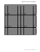
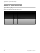
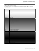
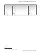
Table 51. I/O Address Map
Address (Hex) Device
0000–000F DMA 1
0020–0021 Interrupt controller 1
0040–0043 Timer 1
0048–004B Timer 2
0060 Keyboard controller data byte
0061 NMI, speaker control
0064 Keyboard controller command/status byte
0070, bit 7 Enable NMI
0070, bits 6:0 Real-time clock, address
0071 Real-time clock, data
0078 Reserved (system board configuration)
007C Reserved (system board configuration)
0080–008F DMA page register
00A0–00A1 Interrupt controller 2
00C0–00DE DMA 2
00F0 Reset numeric error
0170–0177 Secondary IDE channel
01F0–01F7 Primary IDE channel
0278–027B Parallel port 2
02F8–02FF Onboard serial port 2
0376 Secondary IDE channel command port
0377 Secondary IDE channel status port
0378–037F Parallel port 1
03BC–03BF Parallel port x
03E8–03EF Serial port 3
03F0–03F5 Diskette channel 1
03F6 Primary IDE channel command port
03F7 (Write) Diskette channel 1 command
03F7, bit 7 Diskette change channel 1
03F7, bits 6:0 Primary IDE channel status port
03F8–03FF Onboard serial port 1
LPT + 400h ECP port, LPT + 400h
0CF8–0CFB PCI configuration address register
0CFC–0CFF PCI configuration data register
FF00–FF07 IDE bus master register
Appendix B. System Address Maps 43