
Datasheet


CP2102/9
Rev. 1.8 9
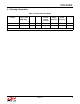
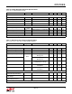
Table 6. Voltage Regulator Electrical Specifications
–40 to +85 °C unless otherwise specified.
Parameter Symbol Test Condition Min Typ Max Unit
CP2102
Input Voltage Range
V
REGIN
4.0 — 5.25 V
Output Voltage
V
DDOUT
Output Current = 1 to 100 mA* 3.0 3.3 3.6 V
VBUS Detection Input Threshold
V
VBUSTH
1.0 1.8 2.9 V
Bias Current
—90—µA
CP2109
Input Voltage Range
V
REGIN
3.0 — 5.25 V
Output Voltage
V
DDOUT
Output Current = 1 to 100 mA* 3.3 3.45 3.6 V
VBUS Detection Input Threshold
V
VBUSTH
2.5 — — V
Bias Current
—8399µA
*Note: The maximum regulator supply current is 100 mA.
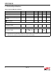
Table 7. USB Transceiver Electrical Specifications
V
DD
= 3.0 V to 3.6 V, –40 to +85 °C unless otherwise specified.
Parameter Symbol Test Condition Min Typ Max Unit
Transmitter
Output High Voltage
V
OH
2.8 — — V
Output Low Voltage
V
OL
——0.8V
Output Crossover Point
V
CRS
1.3 — 2.0 V
Output Impedance (CP2102)
Z
DRV
Driving High
Driving Low
—
—
38
38
—
—
Output Impedance (CP2109)
Driving High
Driving Low
—
—
36
36
—
—
Pull-up Resistance
R
PU
Full Speed (D+ Pull-up)
Low Speed (D- Pull-up)
1.425 1.5 1.575 k
Output Rise Time
T
R
Low Speed
Full Speed
75
4
—
—
300
20
ns
Output Fall Time
T
F
Low Speed
Full Speed
75
4
—
—
300
20
ns
Receiver
Differential Input Sensitivity
V
DI | (D+) - (D-) | 0.2 — — V
Differential Input Common
Mode Range
V
CM 0.8 — 2.5 V
Input Leakage Current
I
L Pullups Disabled — < 1.0 — µA
*Note: Refer to the USB Specification for timing diagrams and symbol definitions.