
Datasheet


CP2102/9
Rev. 1.8 23
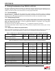
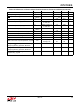
RST Input High Voltage, Minimum
V
IHRESET
0.7 x V
DD
0.75 x V
DD
V
RST
Input Low Voltage, Maximum
V
ILRESET
0.25 x V
DD
0.6 V
Regulator Input Voltage Range, Minimum
V
REGIN
4.0 3.0 V
Regulator Output Voltage, Minimum
V
DDOUT
Output Current = 1
to 100 mA*
3.0 3.3 V
Regulator Output Voltage, Typical
V
DDOUT
Output Current = 1
to 100 mA*
3.3 3.45 V
VBUS Detection Input Threshold, Minimum
V
VBUSTH
1.0 2.5 V
VBUS Detection Input Threshold, Typical
V
VBUSTH
1.8 — V
VBUS Detection Input Threshold, Maximum
V
VBUSTH
2.9 — V
Regulator Bias Current, Typical
90 83 µA
Regulator Bias Current, Maximum
—99µA
USB Transceiver Output Impedance, Typical
Z
DRV
Driving High
Driving Low
38
38
36
36
Ω
Voltage on V
PP
with respect to GND during a
ROM programming operation, Minimum
V
DD
> 3.3 V — 5.75 V
Voltage on V
PP
with respect to GND during a
ROM programming operation, Maximum
V
DD
> 3.3 V — V
DD
+ 3.6 V
Capacitor on V
PP
for In-application
Programming, Typical
—4.7µF
Table 15. Differences in Electrical Specifications between CP2102 and CP2109 (Continued)
Parameter Symbol Test Condition CP2102 CP2109 Unit