
Datasheet


CP2102/9
22 Rev. 1.8
11. Porting Considerations from CP2102 to CP2109
This section highlights the differences between the CP2102 and CP2109. These devices are designed to be pin-
compatible, and thus require very minor changes when porting hardware between devices. The CP2109 is an
updated, cost-reduced version of the CP2102 with a one-time programmable ROM.
11.1. Pin-Compatibility
The CP2109 is pin-compatible with the CP2102 with a single exception; the CP2109 requires an additional
capacitor between V
PP
and GND for in-application programming. This capacitor is not required after the CP2109
EPROM has been successfully programmed or if the CP2109 does not need to be customized in system.
11.2. Distinguishing Factors
The CP2102 has 1024 bytes of EEPROM for vendor ID (VID), product ID (PID), serial number, power descriptor,
release number, and product description strings. This configuration EEPROM can be written and re-written multiple
times. The CP2109 has 1024 bytes of one-time programmable EPROM for configuration. This configuration
EPROM can only be written one time.
The CP2109 may require an additional capacitor on V
PP
if in-application programming is desired.
The CP2102 default serial number is always “0001”. Every CP2109 is programmed from the factory with a unique
serial number.
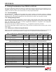
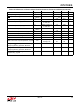
11.3. Differences in Electrical Specifications
Table 14 and Table 15 list differences in absolute maximum and electrical specifications between the CP2102 and
CP2109. Refer to "3. Electrical Specifications" on page 6 for the comprehensive electrical specifications.
Table 14. Differences in Absolute Maximum Specifications between CP2102 and CP2109
Parameter Symbol Test Condition CP2102 CP2109 Unit
Voltage on any I/O Pin, VBUS, or RST with
respect to GND, Maximum
V
DD
> 3.0 V
V
DD
not powered
5.8
5.8
5.8
V
DD
+ 3.6
V
Table 15. Differences in Electrical Specifications between CP2102 and CP2109
Parameter Symbol Test Condition CP2102 CP2109 Unit
Supply Current—Normal, Typical
I
REGIN
Normal Operation;
V
REG
Enabled
20 17 mA
Supply Current—Normal, Maximum
I
REGIN
Normal Operation;
V
REG
Enabled
26 23 mA
Supply Current—Suspended, Typical
I
REGIN
Bus Powered;
V
REG
Enabled
80 90 µA
Supply Current—Suspended, Maximum
I
REGIN
Bus Powered;
V
REG
Enabled
100 230 µA
Output High Voltage, Minimum
V
OH
I
OH
=–3mA V
DD
–0.7 V
DD
–0.2 V
Output High Voltage, Typical
V
OH
I
OH
=–10mA V
DD
–0.8 V
DD
–0.4 V
Output Low Voltage, Maximum
V
OL
I
OL
= 8.5 mA 0.6 0.4 V
Output Low Voltage, Typical
V
OL
I
OL
=25mA 1.0 0.6 V
Input High Voltage, Minimum
V
IH
2.0 0.7 x V
DD
V
Input Low Voltage, Maximum
V
IL
0.8 0.6 V