
Datasheet


5. ELECTRICAL CHARACTERISTICS
5. Electrical Characteristics
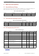
5.1 Absolute Maximum Ratings
Stresses beyond the absolute maximum ratings listed in the table below may cause permanent damage to the
device. These are stress ratings only, and do not refer to the functional operation of the device.
Table 5: Absolute Maximum Ratings
Symbol Parameter Min Max Unit
VDD33 - –0.3 3.6 V
T
store
Storage temperature –40 150 °C
5.2 Recommended Operating Conditions
Table 6: Recommended Operating Conditions
Symbol Parameter Min Typical Max Unit
VDD33 - 2.7 3.3 3.6 V
I
V DD
Current delivered by external power supply 0.5 - - A
T Operating temperature –40 - 85 °C
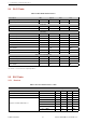
5.3 DC Characteristics (3.3V, 25°C)
Table 7: DC Characteristics
Symbol Parameter Min Typ Max Unit
C
IN
Pin capacitance - 2 - pF
V
IH
High-level input voltage 0.75 × VDD
1
- VDD + 0.3 V
V
IL
Low-level input voltage –0.3 - 0.25 × VDD V
I
IH
High-level input current - - 50 nA
I
IL
Low-level input current - - 50 nA
V
OH
High-level output voltage 0.8 × VDD - - V
V
OL
Low-level output voltage - - 0.1 × VDD V
I
OH
High-level source current (VDD = 3.3V, V
OH
=
2.64V, PAD_DRIVER = 3)
- 40 - mA
I
OL
Low-level sink current (VDD = 3.3V, V
OL
=
0.495V, PAD_DRIVER = 3)
- 28 - mA
R
P U
Pull-up resistor - 45 - kΩ
R
P D
Pull-down resistor - 45 - kΩ
V
IL_nRST
Low-level input voltage of EN to reset the mod-
ule
- - 0.6 V
1. VDD is the I/O voltage for a particular power domain of pins. More details can be found in Appendix IO_MUX of
ESP32 Datasheet.
Espressif Systems 9 ESP32-WROOM-32 Datasheet V2.5