
Datasheet


MB85RS64V
2 DS501-00015-4v0-E
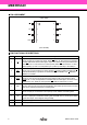
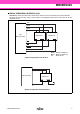
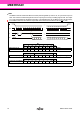
PIN ASSIGNMENT
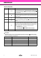
PIN FUNCTIONAL DESCRIPTIONS
Pin No. Pin Name Functional description
1 CS
Chip Select pin
This is an input pin to make chip select. When CS is the “H” level, device is in deselect
(standby) status and SO becomes High-Z. Inputs from other pins are ignored at this time.
When CS is the “L” level, device is in select (active) status. CS has to be the “L” level
before inputting op-code. The Chip Select pin is pulled up internally to the VDD pin.
3 WP
Write Protect pin
This is a pin to control writing to a status register. The writing of status register (see “
STATUS REGISTER”) is protected in related with WP and WPEN. See “ WRITING
PROTECT” for detail.
7 HOLD
Hold pin
This pin is used to interrupt serial input/output without making chip deselect. When
HOLD is the “L” level, hold operation is activated, SO becomes High-Z, and SCK and SI
become don’t care. While the hold operation, CS shall be retained the “L” level.
6 SCK
Serial Clock pin
This is a clock input pin to input/output serial data. SI is loaded synchronously to a rising
edge, SO is output synchronously to a falling edge.
5 SI
Serial Data Input pin
This is an input pin of serial data. This inputs op-code, address, and writing data.
2 SO
Serial Data Output pin
This is an output pin of serial data. Reading data of FRAM memory cell array and status
register are output. This is High-Z during standby.
8 VDD Supply Voltage pin
4 GND Ground pin
GND SI
SO
VDD
SCK
WP
CS
HOLD
8
7
6
54
3
2
1
(TOP VIEW)
(FPT-8P-M02)