
Datasheet

MPL3115A2
Sensors
Freescale Semiconductor, Inc. 9
3.2 Absolute Maximum Ratings
Stresses above those listed as “absolute maximum ratings” may cause permanent damage to the device. This is a stress rating
only and functional operation of the device under these conditions is not implied. Exposure to maximum rating conditions for ex-
tended periods may affect device reliability.
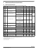
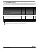
Table 5. Maximum Ratings
Characteristic Symbol Value Unit
Maximum Applied Pressure P
max
500 kPa
Supply Voltage V
DD
-0.3 to 3.6 V
Interface Supply Voltage V
DDIO
-0.3 to 3.6 V
Input Voltage on any Control Pin (SCL, SDA) VIN -0.3 to V
DDIO
+ 0.3 V
Operating Temperature Range T
OP
-40 to +85 °C
Storage Temperature Range T
STG
-40 to +125 °C
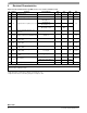
Table 6. ESD And Latch-up Protection Characteristics
Rating Symbol Value Unit
Human Body Model HBM ±2000 V
Machine Model MM ±200 V
Charge Device Model CDM ±500 V
Latch-up Current at T = 85 °C — ±100 mA
This is a mechanical shock sensitive device, improper handling can cause permanent damage to the part or
cause the part to otherwise fail.
This is an ESD sensitive device, improper handling can cause permanent damage to the part.