
Datasheet

MPL3115A2
Sensors
Freescale Semiconductor, Inc. 7
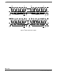
3.1 I
2
C Interface Characteristics
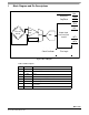
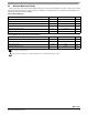
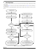
Figure 3. I
2
C Slave Timing Diagram
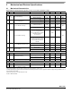
Table 4. I
2
C Slave Timing Values
(1)
1. All values referred to VIH(min) and VIL(max) levels.
Ref Symbol Parameter
I
2
C
Unit
Condition Min Max
1f
SCL
SCL Clock Frequency Pull-up = 1 kΩ, C
b
= 400 pF 0 400 KHz
2f
SCL
SCL Clock Frequency Pull-up = 1 kΩ, C
b
= 20 pF 0 4 MHz
3t
BUF
Bus free time between STOP and START condition 1.3 µs
4t
HD;STA
Repeated START Hold Time 0.6 µs
5t
SU;STA
Repeated START Setup Time 0.6 µs
6t
SU;STO
STOP Condition Setup Time 0.6 µs
7t
HD;DAT
SDA Data Hold Time
(2)
2. t
HD;DAT
is the data hold time that is measured from the falling edge of SCL, applies to data in transmission and the acknowledge.
50
(3)
3. The device must internally provide a hold time of at least 300 ns for the SDA signal (with respect to the VIH(min) of the SCL signal) to bridge
the undefined region of the falling edge of SCL.
(4)
4. The maximum t
HD;DAT
must be less than the maximum of t
VD;DAT
or t
VD;ACK
by a transition time. This device does not stretch the LOW period
(t
LOW)
of the SCL signal.
ns
8t
SU;DAT
SDA Setup Time 100
(5)
5. A fast mode I
2
C device can be used in a standard mode I
2
C system, but the requirement t
SU;DAT
250 ns must then be met. This will
automatically be the case if the device does not stretch the LOW period of the SCL signal. If such a device does stretch the LOW period of
the SCL signal, it must output the next data bit to the SDA line t
r
(max) + t
SU;DAT
= 1000 + 250 = 1250 ns (according to the standard mode I
2
C
specification) before the SCL line is released. Also the acknowledge timing must meet this set-up time.
ns
9t
LOW
SCL Clock Low Time 1.3 µs
10 t
HIGH
SCL Clock High Time 0.6 µs
11 t
r
SDA and SCL Rise Time 20 + 0.1C
b
(6)
6. C
b
= Total capacitance of one bus line in pF.
300 ns
12 t
f
SDA and SCL Fall Time
(3)(6)(7)(8)
7. The maximum t
f
for the SDA and SCL bus lines is specified at 300 ns. The maximum fall time for the SDA output stage t
f
is specified at 250 ns.
This allows series protection resistors to be connected in between the SDA and the SCL pins and the SDA/SCL bus lines without exceeding
the maximum specified t
f
.
8. In Fast Mode Plus, fall time is specified the same for both output stage and bus timing. If series resistors are used, designers should allow for
this when considering bus timing.
20 + 0.1C
b
(6)
300 ns
13 t
SP
Pulse width of spikes that are suppressed by internal
input filter
50 ns