
Datasheet


www.vishay.com Document Number: 81733
2 Rev. 1.5, 04-Feb-11
TSOP382.., TSOP384.., TSOP392.., TSOP394..
Vishay Semiconductors
IR Receiver Modules for Remote
Control Systems
Note
• Stresses beyond those listed under “Absolute Maximum Ratings” may cause permanent damage to the device. This is a stress rating only
and functional operation of the device at these or any other conditions beyond those indicated in the operational sections of this specification
is not implied. Exposure to absolute maximum rating conditions for extended periods may affect the device reliability.
TYPICAL CHARACTERISTICS (T
amb
= 25 °C, unless otherwise specified)
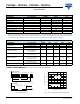
Fig. 1 - Output Active Low Fig. 2 - Pulse Length and Sensitivity in Dark Ambient
ABSOLUTE MAXIMUM RATINGS
PARAMETER TEST CONDITION SYMBOL VALUE UNIT
Supply voltage V
S
- 0.3 to + 6 V
Supply current I
S
3mA
Output voltage V
O
- 0.3 to (V
S
+ 0.3) V
Output current I
O
5mA
Junction temperature T
j
100 °C
Storage temperature range T
stg
- 25 to + 85 °C
Operating temperature range T
amb
- 25 to + 85 °C
Power consumption T
amb
85 °C P
tot
10 mW
Soldering temperature t 10 s, 1 mm from case T
sd
260 °C
ELECTRICAL AND OPTICAL CHARACTERISTICS (T
amb
= 25 °C, unless otherwise specified)
PARAMETER TEST CONDITION SYMBOL MIN. TYP. MAX. UNIT
Supply current
E
v
= 0, V
S
= 3.3 V I
SD
0.27 0.35 0.45 mA
E
v
= 40 klx, sunlight I
SH
0.45 mA
Supply voltage V
S
2.5 5.5 V
Transmission distance
E
v
= 0, test signal see fig. 1,
IR diode TSAL6200,
I
F
= 250 mA
d45m
Output voltage low
I
OSL
= 0.5 mA, E
e
= 0.7 mW/m
2
,
test signal see fig. 1
V
OSL
100 mV
Minimum irradiance
Pulse width tolerance:
t
pi
- 5/f
o
< t
po
< t
pi
+ 6/f
o
,
test signal see fig. 1
E
e min.
0.15 0.35 mW/m
2
Maximum irradiance
t
pi
- 5/f
o
< t
po
< t
pi
+ 6/f
o
,
test signal see fig. 1
E
e max.
30 W/m
2
Directivity
Angle of half transmission
distance
1/2
± 45 deg
E
e
T
t
pi
*
t
* t
pi
10/f
0
is recommended for optimal function
V
O
V
OH
V
OL
t
16110
Optical Test Signal
(IR diode TSAL6200, I
F
= 0.4 A, 30 pulses, f = f
0
, t = 10 ms)
Output Signal
t
d
1)
t
po
2)
1)
7/f
0
< t
d
< 15/f
0
2)
t
pi
- 5/f
0
< t
po
< t
pi
+ 6/f
0
0
0.1
0.2
0.3
0.4
0.5
0.6
0.7
0.8
0.9
1.0
0.1 1 10 10
2
10
3
10
4
10
5
E
e
- Irradiance (mW/m
2
)
t
po
- Output Pulse Width (ms)
20752
Input Burst Length
λ
= 950 nm,
Optical Test Signal, Fig.1
Output Pulse Width