
Data Sheet
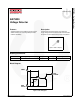
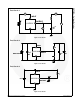
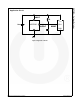
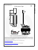

KA75330 — Voltage Detector
© 2002 Fairchild Semiconductor Corporation www.fairchildsemi.com
KA75330 Rev. 1.1.0 2
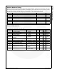
Absolute Maximum Ratings
Stresses exceeding the absolute maximum ratings may damage the device. The device may not function or be opera-
ble above the recommended operating conditions and stressing the parts to these levels is not recommended. In addi-
tion, extended exposure to stresses above the recommended operating conditions may affect device reliability. The
absolute maximum ratings are stress ratings only. Values are at T
A
= 25°C unless otherwise noted.
Electrical Characteristics
Values are at T
A
= 25°C unless otherwise noted.
Symbol Parameter Value Unit
V
CC
Supply Voltage 0.3 ~ +15.0 V
V
DET
Detecting Voltage 3.3 V
V
HYS
Hysteresis Voltage 50 mV
T
OPR
Operating Temperature -25 ~ +85 °C
T
STG
Storage Temperature -50 ~ +150 °C
P
D
Power Dissipation (TO-92) 200 mW
DV
DET
/DT Detecting Voltage Temperature Coefficient R
L
= 200 Ω,+0.01 %/°C
Symbol Parameter Conditions Min. Typ. Max. Unit
V
DET
Detecting Voltage R
L
= 200 Ω, V
OL
≤ 0.4 V 3.15 3.30 3.45 V
V
OL
Low Output Voltage R
L
= 200 Ω 0.4 V
I
LKG
Output Leakage Current V
CC
= 15 V 0.1 μA
V
HYS
Hysteresis Voltage R
L
= 200 Ω 30 50 100 mV
DV
DET
/DT
Detecting Voltage Temperature
Coefficient
R
L
= 200 Ω ±0.01 %/°C
I
CCL
Circuit Current (At On Time) V
CC
= V
DET(MIN)
- 0.05 V 300 500 μA
I
CCH
Circuit Current (At Off Time) V
CC
= 5.25 V 30 50 μA
V
TH(OPR)
Threshold Operating Voltage R
L
= 200 Ω, V
OL
≤ 0.4 V 0.8 1.0 V
t
OL
" L" ± Transmission Delay R
L
= 1.0 kΩ, C
L
= 100 pF 0.6 10 μs
t
OH
" H" ± Transmission Delay R
L
= 1.0 kΩ, C
L
= 100 pF 15 20 μs
I
OLI
Output Current (At On Time)
V
CC
= V
DET(MIN)
- 0.05 V,
T
A
= 25°C
10 20 30 mA
I
OLII
Output Current (At On Time)
V
CC
= V
DET(MIN)
- 0.05 V,
T
A
= -25 ~ +85°C
81630mA