Speedster22i Clock and Reset Networks User Guide UG027 – May 21, 2014 UG027, May 21, 2014 1
Copyright Info Copyright © 2014 Achronix Semiconductor Corporation. All rights reserved. Achronix is a trademark and Speedster is a registered trademark of Achronix Semiconductor Corporation. All other trademarks are the property of their prospective owners. All specifications subject to change without notice. NOTICE of DISCLAIMER: The information given in this document is believed to be accurate and reliable.
Table of Contents Copyright Info .................................................................................................... 2 Table of Contents .............................................................................................. 3 Introduction ....................................................................................................... 4 Clock and Reset Networks Overview .....................................................................................
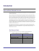
Introduction Clock and Reset Networks Overview Speedster22iHD FPGAs have two hierarchical clock networks: a core clock network and a boundary clock network. The core clock network is the hierarchical network that feeds resources in the FPGA fabric. There are two types of core clock networks: a global and a direct. Both of them have common input sources: Clock input pins and PLL outputs which make up the Clock Generator (CG) and recovered SerDes input clocks.
Reset Resource Counts The following table lists the reset resources available on Speedster22iHD FPGAs.
Clock Sources As mentioned earlier, the clock sources are Clock Generators (CGs) and recovered SerDes input clocks. There are four CGs on a Speedster 22iHD FPGA, one in each corner of the device. Each CG contains six clock I/O buffers (CBs) and four Phase Locked Loops (PLLs). The clock buffers can be used differential I/Os or single‐ended I/Os. If these I/Os are not used as clock buffers, they can be used as generic inputs or outputs.
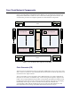
Core Clock Network This chapter focuses solely on the core clock network, illustrating the global and direct core clock network hierarchies and providing a more in-depth look at the different components that make up these networks. Global and Direct Core Clock Network Global Core Clock Network The global core clock network is a balanced and low-skew H-tree that enables clock distribution to all parts of the Speedster 22iHD FPGA fabric.
GCG SerDes GPIO GCG GCG GPIO SerDes GCG Figure 1: Global Core Clock Network Direct Core Clock Network The direct core clock network is a distribution system that provides for much lower clock insertion delay, which is particularly useful for more complex designs that utilize multiple clocks and require clocks to be internally generated and re-distributed to certain parts of the FPGA fabric. Each branch of the direct clock network is restricted to the clock region it reaches.
GCG SerDes GPIO GCG GCG GPIO SerDes GCG Figure 2: Direct Core Clock Network UG027, May 21, 2014 9
Core Clock Network Components Figure 3 provides block level highlights of the different core clock network components on the Speedster 22iHD FPGA. These are color coded to better distinguish between them. The sections below provide more in depth explanations of these different components.
Table 3: Snapshot of HD1000 52.
The PLL contains the following major blocks: reference clock divider, feedback divider, sigma-delta modulator, phase rotator with divider, mux to select internal or external feedback signal, phase-frequency detector, charge pump, loop filter and VCO. The input reference clock can be divided by the reference clock divider. The divider ratio (M) range is 1 to 63 with 50% duty-cycle. This PLL only supports reference clock range of 30MHz to 400MHz (after reference clock divider frequency).
The PLL IP comes with a built-in LDO and a Band Gap reference circuit. The LDO takes external analog voltage (PA_VDD, 1.5V to 1.8V) and generates internal analog voltage to provide cleaner supply voltage to PLL. The Band Gap reference circuit provides the reference voltage for the LDO. In order to calibrate the Band Gap reference and the LDO, without requiring an analog pin, a built-in ADC reference is included in the PLL block as well.
On the other hand, the “Advanced PLL” gives users much more flexibility in setting up the individual PLL parameters, settings, counter values etc. and gives the user full control over exactly how the PLL is tuned. Obviously, in the case of the “Advanced PLL”, it is the user’s responsibility to ensure that the settings provided match the intended behavior.
into the clock hub. Figure 6 below provides a detailed view of the internals of the clock mux located at the top center of the device.
From Clock Mux Top Global Core Clk 32 Direct Core Clk To Clock Region W1 12 To Clock Region W2 12 48 48 12 48 48 12 To Clock Region E1 To Clock Region E2 H-Tree Clock Hub From data interconnect in fabric 80 to 48 Crossbar 16 48 48 To Clock Region Wn-1 12 48 12 48 To Clock Region Wn 12 48 12 To Clock Region En-1 To Clock Region En 32 From Clock Mux Bottom Figure 7: Detailed View of the Clock Hub Clock Region Clock regions in Speedster 22iHD FPGAs have fixed heights, such that a DDR
MULTs LRAMs BRAMs RLBs MULTs RLBs BRAMs RLBs MULTs LRAMs BRAMs RLBs MULTs RLBs BRAMs RLBs MULTs LRAMs BRAMs RLBs MULTs RLBs BRAMs RLBs Clock Region 16 CRMU 48 Global Clocks from Clock Hub 16 From data interconnect in fabric 12 MULTs LRAMs BRAMs RLBs MULTs RLBs BRAMs RLBs MULTs LRAMs BRAMs RLBs MULTs RLBs BRAMs RLBs MULTs LRAMs BRAMs RLBs MULTs RLBs BRAMs RLBs Direct Clocks from Clock Mux Figure 8: Detailed View a Clock Region Clock Region Management
From data interconnect in fabric Global Core Clocks from Clock Hub 24 2 Direct Core Clocks from Clock Mux 16 6 Additional Control Logic 32 to 8 Crossbar Clk Div & Gating 8 8 To Fabric Columns 16 CRMU Clk Div & Gating 8 Global Core Clocks from Clock Hub 24 2 Direct Core Clocks from Clock Mux 8 32 to 8 Crossbar Additional Control Logic 6 From data 16 interconnect in fabric Figure 9: Detailed View of a Clock Region Management Unit (CRMU) Figure 10 below provides a more in-depth look at t
Junctions Data-to-Clock Junctions There are multiple junction-points in the fabric where a data-interconnect signal can drive a clock network signal: a. b. c. d. Clock Hub (16 data inputs; already discussed above), CRMU (4 data inputs per region; already discussed above), RLB input (any Logic Cluster clock can be driven by a selected data signal), Selected BRAM, LRAM, or Multiplier input.
Byte-Lane Clocks For source synchronous transfers, where data and clock are both sent from the IO ring to the core, using one of the clock networks as described above would result in a large skew between the data and the clock. For this reason, there is a dedicated entry point from the byte lanes into the clock inputs of the clock regions, via the data interconnect route in the fabric into the CRMU.
Boundary Clock Network The boundary clock network is an architectural feature available in Speedster22iHD FPGAs to help improve IO ring performance in high speed applications. There are two variants of the boundary clock network: The first is a global boundary clock network, which ensures that clocks coming in from all 4 sides of the device traverse a muxing network that provides for low skew between them.
Global Clock Mux (GCM) Quadrant Clock Mux (QCM) Region Clock Mux (RCM) Byte-Lane Clock Mux (BCM) The global boundary clock network traverses through each of these mux stages, whereas the local boundary clock uses a shortened path that ties the output of the GCM directly into the BCM.
Clock Setting and Reporting Much of the decision making and optimization for clock selection is automatically done by the ACE tool to prevent no-routes. However, ACE does provide users with some options to specify the type of clock networks they wish to use for particular implementations. The clock type can be specified for a particular CG output in the sdc file as shown below. The three options available are: {trunk, direct_trunk, boundary}.
Reset Network This chapter examines the reset network in a little more detail and provides information on the different networks, reset sources as well as associated circuitry in Speedster22i FPGAs. Reset Sources and the Reset Input Block Each corner of a Speedster22i FPGA has an individual Reset Input Block. This block receives external reset inputs as well as inputs generated internally within the device.
and (b) even if it did the user wouldn’t be able to do anything to fix timing problems in the I/O ring. For resets going into the FPGA fabric, the guideline is to use logic in the fabric to ensure that the resets can be synchronized to the particular clock domains. One way of doing this is shown in Figure 15 below, whereby the logic enables going into reset asynchronously, but coming out of it asynchronously.
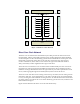
Port_Name DIFF-PAIR USE BANK PURPOSE CLK/RST USE pad0_clk_bank_se pad0_clk_bank_sw pad1_clk_bank_ne pad1_clk_bank_nw pad1_clk_bank_se pad1_clk_bank_sw pad2_clk_bank_ne pad2_clk_bank_nw pad2_clk_bank_se pad2_clk_bank_sw pad3_clk_bank_ne pad3_clk_bank_nw pad3_clk_bank_se pad3_clk_bank_sw pad4_clk_bank_ne pad4_clk_bank_nw pad4_clk_bank_se pad4_clk_bank_sw pad5_clk_bank_ne pad5_clk_bank_nw pad5_clk_bank_se pad5_clk_bank_sw P P N N N N P P P P N N N N P P P P N N N N C C C C C C C C C C C C C C C C C C C
8 bit P Reset source P P Reset source P P P P P Logic Block 8 bit P P 8 bit Logic Block P P 8 bit P P Logic Block P Logic Block P P P P P FPGA Core P Logic Block P P P Logic Block P Programmable Pipeline P P P P P 8 bit Logic Block P Reset source P P 8 bit P P P 8 bit Logic Block P P Reset source P P 8 bit Figure 16: IO Ring Reset Network UG027, May 21, 2014 27
Revision History The following table shows the revision history for this document. 28 Date Version 04/05/2013 05/22/2013 06/07/2013 1.0 1.1 1.2 04/24/2014 1.3 05/01/2014 05/21/2014 1.4 1.5 Revisions Initial Achronix release. Incorporated additional inputs from engineering. Updated PLL description and diagrams. Updated byte-lane clocks. Added in boundary clock network and settings sections. Corrected clock sources. Updated PLL specs. Added information about PLL cascading.