
User manual
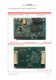

Table Of Contents

Quick Start
SYS_Quick Start_AX_SPU_1.0
2 Getting started
2.1 Start Design
A small test project (/documentation/quickstart/AXSPU_test_fpga) is available for
getting started.
You can use this project as a basis to develop your own application. In the test design
all available board pins are used and the LEDs are toggled. The pinfile is located at
AXSPU_test_top.qsf.
2.2 Required
– 3.3 V ± 5% power supply or Breakout board [AX_SPU_BO]
– Test Design (/documentation/quickstart/AXSPU_test_fpga)
– JTAG Programmer USB Blaster Download Cable [USB-DWLD_1] or
[USB-DWLD_2]
– Altera Software Quartus II Web Edition (≥13.01) [QII5V1], [QII5V1_DWLD]
2.3 Steps to follow
1. Connect power to X302 (figure 2, ../documentation/hardware/
schematic/AX_SPU_schematic.pdf) and connect the JTAG programmer to the
board
2. Open the project file .../AXSPU_test_fpga/AXSPU_test_fpga.qpf in the quartus
II software
3. Open the programmer (Tools/Programmer) and choose your programmer under
Hardware Setup
4. The board can be programmed in JTAG mode:
• to program the FPGA use the sof-file
(.../AXSPU_test_fpga/output_files/AXSPU_test_top.sof)
• to program the flash with JTAG indirect programming use the jic-file
(.../AXSPU_test_fpga/output_files/AXSPU_test.jic). When the board is
programmed repower the board. The design will now be loaded from the
flash.
The sof-file can be converted to a jic-file in the quartus II software
(File/Convert programming file)
5. After the device is programmed the 4 debug LEDs start to toggle in ascending
order
Further details: [AN-370], [QII5V1]
AX_SPU_QuickStart_1.0.odt Page 6 of 7