
User manual
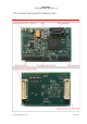

Table Of Contents
Quick Start
SYS_Quick Start_AX_SPU_1.0
1.2 Processing unit
• Altera Cyclone V FPGA 5CEBA2U15 with 25 MHz clock
• Flash memory N25Q032A13ESC as FPGA configuration flash in
active serial single device configuration AS x 4
1.3 IOs
• 36 single ended IOs, up to 6 differential RX and 6 TX pairs, up to 2 external
clock inputs and 1 output on TE connectivity 5179031-1 board to board con-
nectors (X301/ X302)
• 1 LVDS RX and 1 TX pair on SATA connector
• 16 IOs, 2,54 mm pin header (debug connector)
Signals Function
LVDS_RX/ LVDS_RX_CLK LVDS/ LVDS clock receive pair/ single ended IO
IO_T/ LVDS_TX_CLK LVDS/ LVDS clock send pair/ single ended IO
IO single ended IO
Table 1: Signal description
The IO voltage is accessible on the board-to-board connector it can be selected with a
jumper.
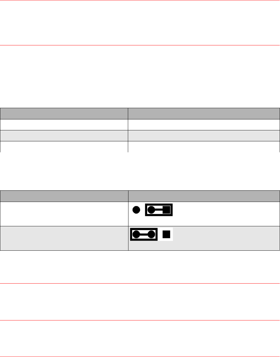
I/O voltage Jumper position
3.3 V
(directly sourced from main supply)
Pin 1 and 2 shorted
2.5 V
(LDO sourced from main supply)
Pin 2 and 3 shorted
Table 2: IO voltage select jumper
For further information concerning IO ressources refer to [CV-52005].
1.4 Further components
• 4 x LED
• Altera FPGA JTAG connector
1.5 Supply voltage and operating conditions
• 3.3 V (±5 %), TE connectivity 5179031-1 or soldering spot
• Temperature Range: Industrial (-40 .. +85 °C) or Commercial (0 .. +70 °C)
AX_SPU_QuickStart_1.0.odt Page 5 of 7