
Data Sheet
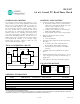
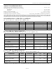
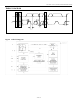
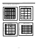
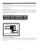
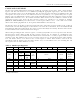
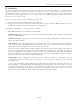
Table Of Contents
- TYPICAL OPERATING CIRCUIT
- PIN CONFIGURATIONS
- ORDERING INFORMATION
- ABSOLUTE MAXIMUM RATINGS
- RECOMMENDED DC OPERATING CONDITIONS
- (TA = 0 C to +70 C, TA = -40 C to +85 C.) (Notes 1, 2)
- DC ELECTRICAL CHARACTERISTICS
- (VCC = 4.5V to 5.5V; TA = 0 C to +70 C, TA = -40 C to +85 C.) (Notes 1, 2)
- DC ELECTRICAL CHARACTERISTICS
- (VCC = 0V, VBAT = 3.0V; TA = 0 C to +70 C, TA = -40 C to +85 C.) (Notes 1, 2)
- AC ELECTRICAL CHARACTERISTICS
- (VCC = 4.5V to 5.5V; TA = 0 C to +70 C, TA = -40 C to +85 C.)
- CAPACITANCE
- (TA = +25 C)
- 64 x 8, Serial, I2C Real-Time Clock
- SYMBOL
- TIMING DIAGRAM
- RS1

DS1307 64 x 8, Serial, I
2
C Real-Time Clock
CLOCK AND CALENDAR
The time and calendar information is obtained by reading the appropriate register bytes. Table 2 shows the RTC
registers. The time and calendar are set or initialized by writing the appropriate register bytes. The contents of the
time and calendar registers are in the BCD format. The day-of-week register increments at midnight. Values that
correspond to the day of week are user-defined but must be sequential (i.e., if 1 equals Sunday, then 2 equals
Monday, and so on.) Illogical time and date entries result in undefined operation. Bit 7 of Register 0 is the clock halt
(CH) bit. When this bit is set to 1, the oscillator is disabled. When cleared to 0, the oscillator is enabled. On first
application of power to the device the time and date registers are typically reset to 01/01/00 01 00:00:00
(MM/DD/YY DOW HH:MM:SS). The CH bit in the seconds register will be set to a 1. The clock can be halted
whenever the timekeeping functions are not required, which minimizes current (I
BATDR
).
The DS1307 can be run in either 12-hour or 24-hour mode. Bit 6 of the hours register is defined as the 12-hour or
24-hour mode-select bit. When high, the 12-hour mode is selected. In the 12-hour mode, bit 5 is the AM/PM bit with
logic high being PM. In the 24-hour mode, bit 5 is the second 10-hour bit (20 to 23 hours). The hours value must be
re-entered whenever the 12/24-hour mode bit is changed.
When reading or writing the time and date registers, secondary (user) buffers are used to prevent errors when the
internal registers update. When reading the time and date registers, the user buffers are synchronized to the
internal registers on any I
2
C START. The time information is read from these secondary registers while the clock
continues to run. This eliminates the need to re-read the registers in case the internal registers update during a
read. The divider chain is reset whenever the seconds register is written. Write transfers occur on the I
2
C
acknowledge from the DS1307. Once the divider chain is reset, to avoid rollover issues, the remaining time and
date registers must be written within one second.
Table 2. Timekeeper Registers
ADDRESS
BIT 7
BIT 6
BIT 5
BIT 4
BIT 3
BIT 2
BIT 1
BIT 0
FUNCTION
RANGE
00h
CH
10 Seconds
Seconds
Seconds
00–59
01h
0
10 Minutes
Minutes
Minutes
00–59
02h 0
12
10
Hour
10
Hour
Hours Hours
1–12
+AM/PM
00–23
24
PM/
AM
03h
0
0
0
0
0
DAY
Day
01–07
04h
0
0
10 Date
Date
Date
01–31
05h 0 0 0
10
Month
Month Month 01–12
06h
10 Year
Year
Year
00–99
07h
OUT
0
0
SQWE
0
0
RS1
RS0
Control
—
08h–3Fh
RAM
56 x 8
00h–FFh
0 = Always reads back as 0.
8 of 14