
Data Sheet
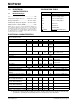
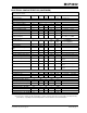

MCP3202
DS21034D-page 4 © 2006 Microchip Technology Inc.
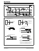
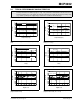
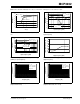
FIGURE 1-1: Serial Timing.
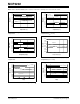
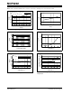
FIGURE 1-2: Test Circuits.
CS
CLK
D
IN MSB IN
t
SU
t
HD
t
SUCS
t
CSH
t
HI
t
LO
D
OUT
t
EN
t
DO
t
R
t
F
LSB
MSB OUT
t
DIS
NULL BIT
V
IH
T
DIS
CS
D
OUT
Waveform 1*
D
OUT
Waveform 2†
90%
10%
* Waveform 1 is for an output with internal conditions such that
the output is high, unless disabled by the output control.
† Waveform 2 is for an output with internal conditions such that
the output is low, unless disabled by the output control.
Voltage Waveforms for t
DIS
Test Point
1.4V
D
OUT
Load circuit for tR, t
F
, t
DO
3kΩ
C
L
= 100 pF
Test Point
D
OUT
Load circuit for t
DIS
and t
EN
3kΩ
100 pF
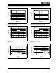
t
DIS
Waveform 2
t
DIS
Waveform 1
CS
CLK
D
OUT
t
EN
12
B11
Voltage Waveforms for t
EN
t
EN
Waveform
V
DD
V
DD
/2
V
SS
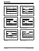
3
4
D
OUT
t
R
Voltage Waveforms for t
R
, t
F
CLK
D
OUT
t
DO
Voltage Waveforms for t
DO
t
F
V
OH
V
OL