
Data Sheet

MCP3202
DS21034D-page 2 © 2006 Microchip Technology Inc.
1.0 ELECTRICAL
CHARACTERISTICS
1.1 Maximum Ratings*
V
DD
.........................................................................7.0V
All inputs and outputs w.r.t. V
SS
...... -0.6V to V
DD
+0.6V
Storage temperature ..........................-65°C to +150°C
Ambient temp. with power applied .....-65°C to +125°C
ESD protection on all pins (HBM)......................... > 4kV
*Notice: Stresses above those listed under “Maximum Ratings” may
cause permanent damage to the device. This is a stress rating only
and functional operation of the device at those or any other conditions
above those indicated in the operational listings of this specification is
not implied. Exposure to maximum rating conditions for extended
periods may affect device reliability.
PIN FUNCTION TABLE
Name Function
V
DD
/V
REF
+2.7V to 5.5V Power Supply and
Reference Voltage Input
CH0 Channel 0 Analog Input
CH1 Channel 1 Analog Input
CLK Serial Clock
D
IN
Serial Data In
D
OUT
Serial Data Out
CS/SHDN Chip Select/Shutdown Input
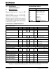
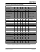
ELECTRICAL CHARACTERISTICS
All parameters apply at V
DD
= 5.5V, V
SS
= 0V, T
AMB
= -40°C to +85°C, f
SAMPLE
= 100 ksps and f
CLK
= 18*f
SAMPLE
unless otherwise noted.
Parameter Sym Min. Typ. Max. Units Conditions
Conversion Rate:
Conversion Time t
CONV
— — 12 clock
cycles
Analog Input Sample Time t
SAMPLE
1.5 clock
cycles
Throughput Rate f
SAMPLE
—
—
—
—
100
50
ksps
ksps
V
DD
= V
REF
= 5V
V
DD
= V
REF
= 2.7V
DC Accuracy:
Resolution 12 bits
Integral Nonlinearity INL —
—
±0.75
±1
±1
±2
LSB
LSB
MCP3202-B
MCP3202-C
Differential Nonlinearity DNL — ±0.5 ±1 LSB No missing codes over
temperature
Offset Error — ±1.25 ±3 LSB
Gain Error — ±1.25 ±5 LSB
Dynamic Performance:
Total Harmonic Distortion THD — -82 — dB V
IN
= 0.1V to 4.9V@1 kHz
Signal to Noise and Distortion
(SINAD)
SINAD — 72 — dB V
IN
= 0.1V to 4.9V@1 kHz
Spurious Free Dynamic Range SFDR — 86 — dB V
IN
= 0.1V to 4.9V@1 kHz
Analog Inputs:
Input Voltage Range for CH0 or
CH1 in Single-Ended Mode
V
SS
—V
DD
V
Input Voltage Range for IN+ in
Pseudo-Differential Mode
IN+ IN- — V
DD
+IN- See Sections 3.1 and 4.1
Input Voltage Range for IN- in
Pseudo-Differential Mode
IN- V
SS
-100 — V
SS
+100 mV See Sections 3.1 and 4.1
Leakage Current — .001 ±1 μA
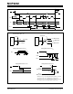
Switch Resistance R
SS
—1k— Ω See Figure 4-1
Note 1: This parameter is established by characterization and not 100% tested.
2: Because the sample cap will eventually lose charge, effective clock rates below 10 kHz can affect linearity
performance, especially at elevated temperatures. See Section 6.2 for more information.