
Data Sheet

MCP3202
DS21034D-page 12 © 2006 Microchip Technology Inc.
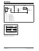
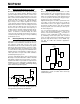
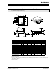
FIGURE 4-1: Analog Input Model.
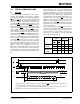
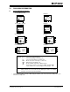
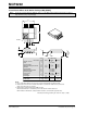
FIGURE 4-2: Maximum Clock Frequency vs. Input
Resistance (R
S
) to maintain less than a 0.1 LSB
deviation in INL from nominal conditions.
C
PIN
VA
R
SS
CHx
7pF
V
T
= 0.6V
V
T
= 0.6V
I
LEAKAGE
Sampling
Switch
SS
R
S
= 1 kΩ
C
SAMPLE
= DAC capacitance
V
SS
V
DD
= 20 pF
±1 nA
Legend
VA = signal source
R
SS
= source impedance
CHx = input channel pad
C
PIN
= input pin capacitance
V
T
= threshold voltage
I
LEAKAGE
= leakage current at the pin
due to various junctions
SS = sampling switch
R
S
= sampling switch resistor
C
SAMPLE
= sample/hold capacitance
0.0
0.2
0.4
0.6
0.8
1.0
1.2
1.4
1.6
1.8
2.0
100 1000 10000
Input Resistance (Ohms)
Clock Frequency (MHz)
V
DD
= 5V
V
DD
= 2.7V