
Data Sheet

PCA9685 All information provided in this document is subject to legal disclaimers. © NXP B.V. 2010. All rights reserved.
Product data sheet Rev. 3 — 2 September 2010 8 of 51
NXP Semiconductors
PCA9685
16-channel, 12-bit PWM Fm+ I
2
C-bus LED controller
7.1.4 Software Reset I
2
C-bus address
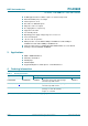
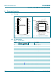
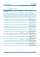
The address shown in Figure 5 is used when a reset of the PCA9685 needs to be
performed by the master. The Software Reset address (SWRST Call) must be used with
R/W
= logic 0. If R/W = logic 1, the PCA9685 does not acknowledge the SWRST. See
Section 7.6 “
Software reset” for more detail.
Remark: The Software Reset I
2
C-bus address is a reserved address and cannot be used
as a regular I
2
C-bus slave address or as an LED All Call or LED Sub Call address.
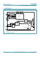
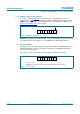
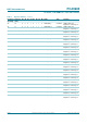
7.2 Control register
Following the successful acknowledgement of the slave address, LED All Call address or
LED Sub Call address, the bus master will send a byte to the PCA9685, which will be
stored in the Control register.
This register is used as a pointer to determine which register will be accessed.
Fig 5. Software Reset address
0
002aab41
6
0 0 0 0 0 1 1
R/W
reset state = 00h
Remark: The Control register does not apply to the Software Reset I
2
C-bus address.
Fig 6. Control register
002aac82
6
D7 D6 D5 D4 D3 D2 D1 D0