
Data Sheet

PCA9685 All information provided in this document is subject to legal disclaimers. © NXP B.V. 2010. All rights reserved.
Product data sheet Rev. 3 — 2 September 2010 38 of 51
NXP Semiconductors
PCA9685
16-channel, 12-bit PWM Fm+ I
2
C-bus LED controller
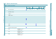
[1] V
DD
must be lowered to 0.2 V in order to reset part.
[2] Each bit must be limited to a maximum of 25 mA and the total package limited to 400 mA due to internal busing limits.
Address inputs; OE input; EXTCLK
V
IL
LOW-level input voltage −0.5 - +0.3V
DD
V
V
IH
HIGH-level input voltage 0.7V
DD
-5.5V
I
LI
input leakage current −1- +1μA
C
i
input capacitance - 3 5 pF
Table 13. Static characteristics
…continued
V
DD
= 2.3 V to 5.5 V; V
SS
=0V; T
amb
=
−
40
°
Cto+85
°
C; unless otherwise specified.
Symbol Parameter Conditions Min Typ Max Unit
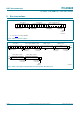
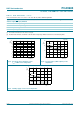
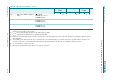
Fig 28. I
DD
typical values with OSC on and
f
SCL
= 1 MHz versus temperature
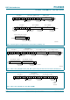
Fig 29. I
OL
typical drive (LEDn outputs) versus
temperature
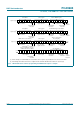
Fig 30. Standby supply current versus temperature
002aad877
T
amb
(°C)
−50 100500
4
6
2
8
10
I
DD
(mA)
0
V
DD
= 5.5 V
3.3 V
2.3 V
−50 100500
002aad878
20
40
60
I
OL
(mA)
0
T
amb
(°C)
V
DD
= 4.5 V
3.0 V
2.3 V
002aad879
T
amb
(°C)
−50 100500
2
3
1
4
5
I
stb
(μA)
0
V
DD
= 5.5 V
3.3 V
2.3 V