
Data Sheet

PCA9685 All information provided in this document is subject to legal disclaimers. © NXP B.V. 2010. All rights reserved.
Product data sheet Rev. 3 — 2 September 2010 33 of 51
NXP Semiconductors
PCA9685
16-channel, 12-bit PWM Fm+ I
2
C-bus LED controller
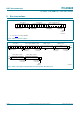
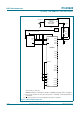
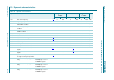
(1) In this example, several PCA9685s are used and the same sequences (A) and (B) above are sent to each of them.
(2) Acknowledge from all the slave devices configured for the new LED All Call I
2
C-bus address in sequence (B).
Fig 25. LED All Call I
2
C-bus address programming and LED All Call sequence example
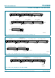
A5 A4 A3 A2 A1 A0 0 AS 1
slave address
START condition R/W
acknowledge
from slave
002aad1
92
0 0 0 0 0 0 00
control register
A
acknowledge
from slave
MODE1
register selection
0 1 0 0 1 1 10
data for MODE1 register
P
STOP
condition
A
acknowledge
from slave
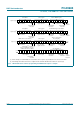
A5 A4 A3 A2 A1 A0 0 AS 1
slave address
START condition R/W
acknowledge
from slave
0 0 0 0 1 0 10
control register
A
acknowledge
from slave
ALLCALLADR
register selection
0 1 0 1 0 1 X1
new LEDALLCALL I
2
C-bus address
P
STOP
condition
A
acknowledge
from slave
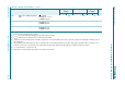
sequence (A)
(1)
sequence (B)
(1)
0 1 0 1 0 1 0 AS 1
LEDALLCALL I
2
C-bus address
START condition R/W
acknowledge
(2)
from all the
devices configured for the new
LEDALLCALL I
2
C-bus address
1 1 1 1 0 1 01
control register
A
acknowledge
(2)
from slave
ALL_LED_ON_L
register selection
0 0 0 0 0 0 00
data for control register
ALL_LED_ON_L
P
STOP
condition
A
acknowledge
(2)
from slave
sequence (C)
(cont.)
(cont.)
0 0 0 0 0 0 0 A0 0 0 0 0 0 0 00 A
acknowledge
(2)
from slave
data for ALL_LED_OFF_L
control register
0 0 0 1 0 0 00 A
acknowledge
(2)
from slave
ALL_LED_ON_H
control register
acknowledge
(2)
from slave
AI on enable ALL CALL
ALL_LED_OFF_H